- 您现在的位置:买卖IC网 > PDF目录11210 > ADUC7061BCPZ32-RL (Analog Devices Inc)IC MCU 16/32BIT 32KB 32LFCSP PDF资料下载
参数资料
| 型号: | ADUC7061BCPZ32-RL |
| 厂商: | Analog Devices Inc |
| 文件页数: | 61/108页 |
| 文件大小: | 0K |
| 描述: | IC MCU 16/32BIT 32KB 32LFCSP |
| 产品变化通告: | ADuC7060/1 Idd Specification Change 01/Feb/2010 |
| 设计资源: | USB Based Temperature Monitor Using ADuC7061 and an External RTD (CN0075) 4 mA-to-20 mA Loop-Powered Temperature Monitor Using ADuC7060/1 (CN0145) |
| 标准包装: | 5,000 |
| 系列: | MicroConverter® ADuC7xxx |
| 核心处理器: | ARM7 |
| 芯体尺寸: | 16/32-位 |
| 速度: | 10MHz |
| 连通性: | I²C,SPI,UART/USART |
| 外围设备: | POR,PWM,温度传感器,WDT |
| 输入/输出数: | 8 |
| 程序存储器容量: | 32KB(16K x 16) |
| 程序存储器类型: | 闪存 |
| RAM 容量: | 1K x 32 |
| 电压 - 电源 (Vcc/Vdd): | 2.375 V ~ 2.625 V |
| 数据转换器: | A/D 5x24b,8x24b,D/A 1x14b |
| 振荡器型: | 内部 |
| 工作温度: | -40°C ~ 125°C |
| 封装/外壳: | 32-VFQFN 裸露焊盘,CSP |
| 包装: | 带卷 (TR) |
第1页第2页第3页第4页第5页第6页第7页第8页第9页第10页第11页第12页第13页第14页第15页第16页第17页第18页第19页第20页第21页第22页第23页第24页第25页第26页第27页第28页第29页第30页第31页第32页第33页第34页第35页第36页第37页第38页第39页第40页第41页第42页第43页第44页第45页第46页第47页第48页第49页第50页第51页第52页第53页第54页第55页第56页第57页第58页第59页第60页当前第61页第62页第63页第64页第65页第66页第67页第68页第69页第70页第71页第72页第73页第74页第75页第76页第77页第78页第79页第80页第81页第82页第83页第84页第85页第86页第87页第88页第89页第90页第91页第92页第93页第94页第95页第96页第97页第98页第99页第100页第101页第102页第103页第104页第105页第106页第107页第108页
ADuC7060/ADuC7061
Data Sheet
Rev. D | Page 56 of 108
DAC PERIPHERALS
DAC
The ADuC706x incorporates a voltage output DAC on chip. In
normal mode, the DAC resolution is 12-bits. In interpolation,
the DAC resolution is 16 bits with 14 effective bits. The DAC
has a rail-to-rail voltage output buffer capable of driving
5 k/100 pF.
The DAC has four selectable ranges.
0 V to VREF (internal band gap 1.2 V reference)
VREF to VREF+
ADC5/EXT_REF2IN to ADC4/EXT_REF2IN+
0 V to AVDD
The maximum signal range is 0 V to AVDD.
Op Amp Mode
As an option, the DAC can be disabled and its output buffer
used as an op amp.
MMR INTERFACE
The DAC is configurable through a control register and a data
register.
DAC0CON Register
Name:
DAC0CON
Address:
0xFFFF0600
Default value:
0x0200
Access:
Read and write
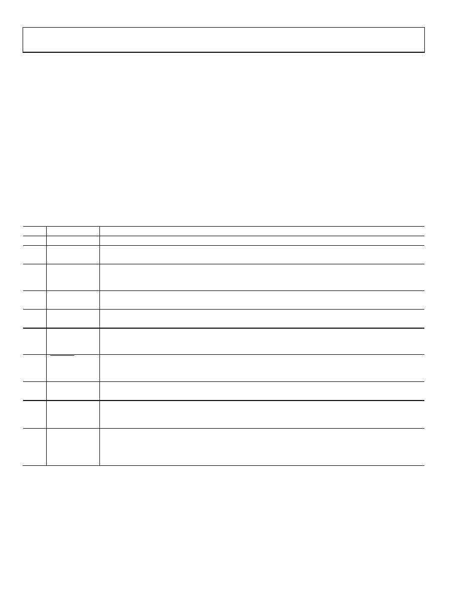
Table 63. DAC0CON MMR Bit Designations
Bit
Name
Description
15:10
Reserved.
9
DACPD
Set to 1 to power down DAC output (DAC output is tristated).
Clear this bit to enable the DAC.
8
DACBUFLP
Set to 1 to place the DAC output buffer in low power mode. See the Normal DAC Mode and Op Amp Mode
sections for further details on electrical specifications.
Clear this bit to enable the DAC buffer.
7
OPAMP
Set to 1 to place the DAC output buffer in op amp mode.
Clear this bit to enable the DAC output buffer for normal DAC operation.
6
DACBUFBYPASS
Set to 1 to bypass the output buffer and send the DAC output directly to the output pin.
Clear this bit to buffer the DAC output.
5
DACCLK
Cleared to 0 to update the DAC on the negative edge of HCLK.
Set to 1 to update the DAC on the negative edge of Timer0. This mode is ideally suited for waveform generation
where the next value in the waveform is written to DAC0DAT at regular intervals of Timer0.
4
DACCLR
Set to 1 for normal DAC operation.
Set to 0 to clear the DAC output and to set DAC0DAT to 0. Writing to this bit has an immediate effect on the DAC
output.
3
DACMODE
Set to 1 to enable the DAC in 16-bit interpolation mode.
Set to 0 to enable the DAC in normal 12-bit mode.
2
Rate
Used with interpolation mode.
Set to 1 to configure the interpolation clock as UCLK/16.
Set to 0 to configure the interpolation clock as UCLK/32.
1:0
DAC range bits
[11] = 0 V to AVDD range.
[10] = ADC5/EXT_REF2IN to ADC4/EXT_REF2IN+.
[01] = VREF to VREF+.
[00] = 0 V to VREF (1.2 V) range. Internal reference source.
相关PDF资料 |
PDF描述 |
|---|---|
| VI-B2L-IW-F4 | CONVERTER MOD DC/DC 28V 100W |
| ATMEGA8535L-8JU | MCU AVR 8K ISP FLASH MEM 44-PLCC |
| VI-B2L-IW-F3 | CONVERTER MOD DC/DC 28V 100W |
| ATMEGA8535L-8PU | IC AVR MCU 8K 8MHZ 3V 40DIP |
| VI-B2L-IW-F2 | CONVERTER MOD DC/DC 28V 100W |
相关代理商/技术参数 |
参数描述 |
|---|---|
| ADUC70SMARTLINKRL7 | 制造商:Analog Devices 功能描述: |
| ADUC70TEL | 制造商:Analog Devices 功能描述:FLASH ARM +5-CH 12BIT ADC - Trays |
| ADUC70TEL-RL7 | 制造商:Analog Devices 功能描述: |
| ADUC7120BBCZ | 制造商:Analog Devices 功能描述:- Rail/Tube |
| ADUC7120BBCZ-RL | 制造商:Analog Devices 功能描述:- Tape and Reel |
发布紧急采购,3分钟左右您将得到回复。