- 您现在的位置:买卖IC网 > PDF目录11210 > ADUC7061BCPZ32-RL (Analog Devices Inc)IC MCU 16/32BIT 32KB 32LFCSP PDF资料下载
参数资料
| 型号: | ADUC7061BCPZ32-RL |
| 厂商: | Analog Devices Inc |
| 文件页数: | 98/108页 |
| 文件大小: | 0K |
| 描述: | IC MCU 16/32BIT 32KB 32LFCSP |
| 产品变化通告: | ADuC7060/1 Idd Specification Change 01/Feb/2010 |
| 设计资源: | USB Based Temperature Monitor Using ADuC7061 and an External RTD (CN0075) 4 mA-to-20 mA Loop-Powered Temperature Monitor Using ADuC7060/1 (CN0145) |
| 标准包装: | 5,000 |
| 系列: | MicroConverter® ADuC7xxx |
| 核心处理器: | ARM7 |
| 芯体尺寸: | 16/32-位 |
| 速度: | 10MHz |
| 连通性: | I²C,SPI,UART/USART |
| 外围设备: | POR,PWM,温度传感器,WDT |
| 输入/输出数: | 8 |
| 程序存储器容量: | 32KB(16K x 16) |
| 程序存储器类型: | 闪存 |
| RAM 容量: | 1K x 32 |
| 电压 - 电源 (Vcc/Vdd): | 2.375 V ~ 2.625 V |
| 数据转换器: | A/D 5x24b,8x24b,D/A 1x14b |
| 振荡器型: | 内部 |
| 工作温度: | -40°C ~ 125°C |
| 封装/外壳: | 32-VFQFN 裸露焊盘,CSP |
| 包装: | 带卷 (TR) |
第1页第2页第3页第4页第5页第6页第7页第8页第9页第10页第11页第12页第13页第14页第15页第16页第17页第18页第19页第20页第21页第22页第23页第24页第25页第26页第27页第28页第29页第30页第31页第32页第33页第34页第35页第36页第37页第38页第39页第40页第41页第42页第43页第44页第45页第46页第47页第48页第49页第50页第51页第52页第53页第54页第55页第56页第57页第58页第59页第60页第61页第62页第63页第64页第65页第66页第67页第68页第69页第70页第71页第72页第73页第74页第75页第76页第77页第78页第79页第80页第81页第82页第83页第84页第85页第86页第87页第88页第89页第90页第91页第92页第93页第94页第95页第96页第97页当前第98页第99页第100页第101页第102页第103页第104页第105页第106页第107页第108页
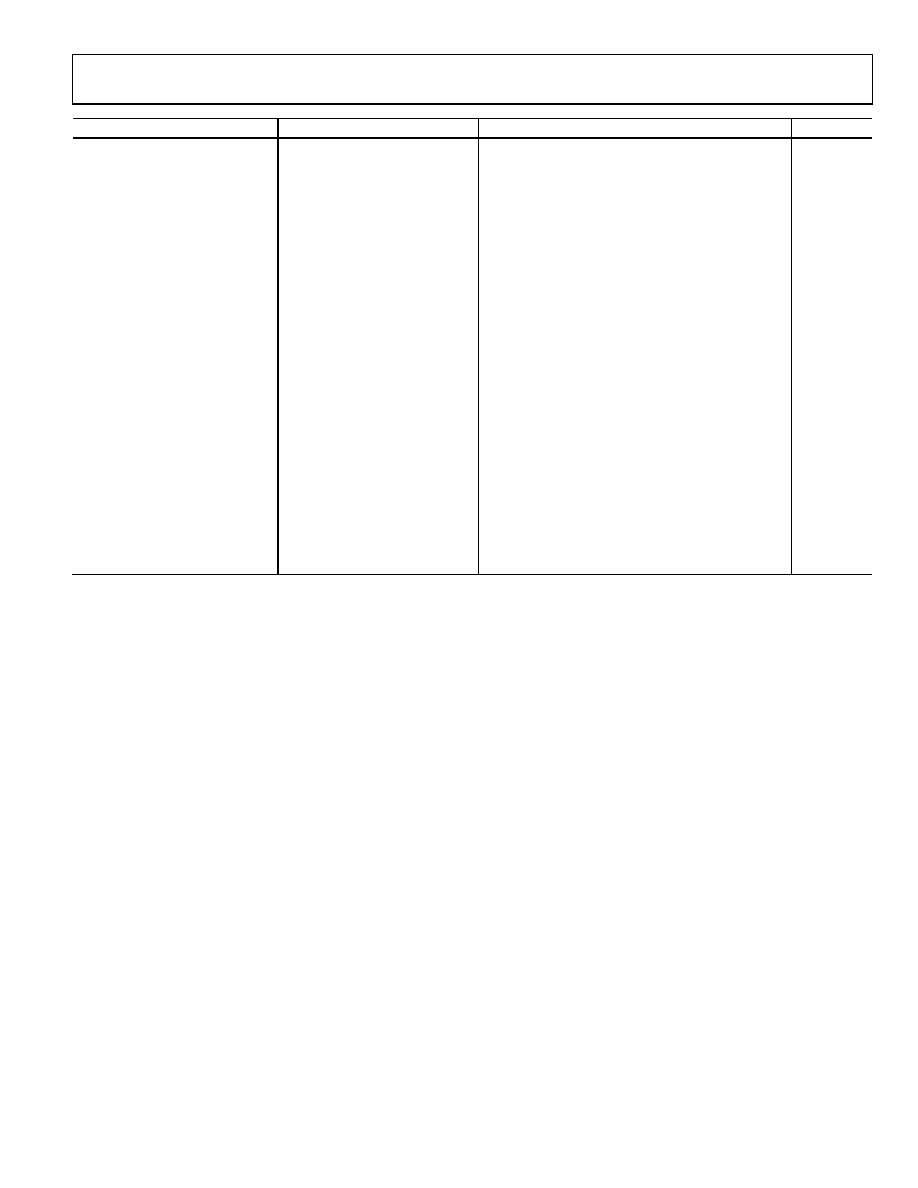
Data Sheet
ADuC7060/ADuC7061
Rev. D | Page 9 of 108
Parameter
Test Conditions/Comments
Min
Typ
Max
Unit
POWER REQUIREMENTS
Power Supply Voltages
DVDD (±5%)
2.375
2.5
2.625
V
AVDD (±5%)
2.375
2.5
2.625
V
Power Consumption
MCU clock rate = 10.24 MHz,
ADC0 on
6
10
mA
MCU clock rate = 640 kHz,
ADC0 on, G = 4, ADC1/DAC off,
SPI on; POWCON1 = 0x4
Full temperature range
3.1
mA
Reduced temperature range
40°C to +85°C1
2.74
mA
Full temperature range
55
350
A
Reduced temperature range
40°C to +85°C
55
120
A
IDD (Primary ADC)
PGA enabled, normal mode/low
power mode; current is
dependent on gain setting
0.6/0.3
mA
ADC0 on, G = 1, normal mode
0.03
mA
ADC0 on, G = 4, normal mode
0.44
mA
ADC0 on, G = >128, normal mode
0.63
mA
IDD (Auxiliary ADC)
Normal mode/low power mode
0.35/0.1
mA
IDD (DAC)
DAC0CON = 0x10
0.33
mA
PWM
0.34
mA
1
These numbers are not production tested but are guaranteed by design and/or characterization data at production release.
2
Valid for primary ADC gain setting of PGA = 4 to 64.
3
Tested at gain range = 4 after initial offset calibration.
4
Measured with an internal short. A system zero-scale calibration removes this error.
5
Measured with an internal short.
6
These numbers do not include internal reference temperature drift.
7
Factory calibrated at gain = 1.
8
System calibration at a specific gain range removes the error at this gain range.
9
Measured using an external reference.
10
Ensure common mode voltage is set so VIN*Gain setting, which is the PGA output voltage, is between 0.1V and VDD – 0.7V. 900 mV is an optimum value for the
common mode voltage across all gains.
11
Measured using the box method.
12
References up to AVDD are accommodated by setting ADC0CON Bit 12.
13
Reference DAC linearity is calculated using a reduced code range of 171 to 4095.
14
Reference DAC linearity is calculated using a reduced code range of 2731 to 65,535.
15
Die temperature.
16
Endurance is qualified to 10,000 cycles as per JEDEC Std. 22 Method A117 and measured at 40°C, +25°C, and +125°C. Typical endurance at 25°C is 170,000 cycles.
17
Retention lifetime equivalent at junction temperature (TJ) = 85°C as per JEDEC Std. 22 Method A117. Retention lifetime derates with junction temperature.
18
Typical additional supply current consumed during Flash/EE memory program and erase cycles is 7 mA and 5 mA, respectively.
相关PDF资料 |
PDF描述 |
|---|---|
| VI-B2L-IW-F4 | CONVERTER MOD DC/DC 28V 100W |
| ATMEGA8535L-8JU | MCU AVR 8K ISP FLASH MEM 44-PLCC |
| VI-B2L-IW-F3 | CONVERTER MOD DC/DC 28V 100W |
| ATMEGA8535L-8PU | IC AVR MCU 8K 8MHZ 3V 40DIP |
| VI-B2L-IW-F2 | CONVERTER MOD DC/DC 28V 100W |
相关代理商/技术参数 |
参数描述 |
|---|---|
| ADUC70SMARTLINKRL7 | 制造商:Analog Devices 功能描述: |
| ADUC70TEL | 制造商:Analog Devices 功能描述:FLASH ARM +5-CH 12BIT ADC - Trays |
| ADUC70TEL-RL7 | 制造商:Analog Devices 功能描述: |
| ADUC7120BBCZ | 制造商:Analog Devices 功能描述:- Rail/Tube |
| ADUC7120BBCZ-RL | 制造商:Analog Devices 功能描述:- Tape and Reel |
发布紧急采购,3分钟左右您将得到回复。