- 您现在的位置:买卖IC网 > PDF目录11210 > ADUC7061BCPZ32-RL (Analog Devices Inc)IC MCU 16/32BIT 32KB 32LFCSP PDF资料下载
参数资料
| 型号: | ADUC7061BCPZ32-RL |
| 厂商: | Analog Devices Inc |
| 文件页数: | 63/108页 |
| 文件大小: | 0K |
| 描述: | IC MCU 16/32BIT 32KB 32LFCSP |
| 产品变化通告: | ADuC7060/1 Idd Specification Change 01/Feb/2010 |
| 设计资源: | USB Based Temperature Monitor Using ADuC7061 and an External RTD (CN0075) 4 mA-to-20 mA Loop-Powered Temperature Monitor Using ADuC7060/1 (CN0145) |
| 标准包装: | 5,000 |
| 系列: | MicroConverter® ADuC7xxx |
| 核心处理器: | ARM7 |
| 芯体尺寸: | 16/32-位 |
| 速度: | 10MHz |
| 连通性: | I²C,SPI,UART/USART |
| 外围设备: | POR,PWM,温度传感器,WDT |
| 输入/输出数: | 8 |
| 程序存储器容量: | 32KB(16K x 16) |
| 程序存储器类型: | 闪存 |
| RAM 容量: | 1K x 32 |
| 电压 - 电源 (Vcc/Vdd): | 2.375 V ~ 2.625 V |
| 数据转换器: | A/D 5x24b,8x24b,D/A 1x14b |
| 振荡器型: | 内部 |
| 工作温度: | -40°C ~ 125°C |
| 封装/外壳: | 32-VFQFN 裸露焊盘,CSP |
| 包装: | 带卷 (TR) |
第1页第2页第3页第4页第5页第6页第7页第8页第9页第10页第11页第12页第13页第14页第15页第16页第17页第18页第19页第20页第21页第22页第23页第24页第25页第26页第27页第28页第29页第30页第31页第32页第33页第34页第35页第36页第37页第38页第39页第40页第41页第42页第43页第44页第45页第46页第47页第48页第49页第50页第51页第52页第53页第54页第55页第56页第57页第58页第59页第60页第61页第62页当前第63页第64页第65页第66页第67页第68页第69页第70页第71页第72页第73页第74页第75页第76页第77页第78页第79页第80页第81页第82页第83页第84页第85页第86页第87页第88页第89页第90页第91页第92页第93页第94页第95页第96页第97页第98页第99页第100页第101页第102页第103页第104页第105页第106页第107页第108页
ADuC7060/ADuC7061
Data Sheet
Rev. D | Page 58 of 108
NONVOLATILE FLASH/EE MEMORY
The ADuC706x incorporates Flash/EE memory technology
on chip to provide the user with nonvolatile, in-circuit reprogram-
mable memory space.
Like EEPROM, flash memory can be programmed in-system
at a byte level, although it must first be erased. The erase is
performed in page blocks. As a result, flash memory is often
and, more correctly, referred to as Flash/EE memory.
Overall, Flash/EE memory represents a step closer to the
ideal memory device that includes nonvolatility, in-circuit
programmability, high density, and low cost. Incorporated in
the ADuC706x, Flash/EE memory technology allows the user
to update program code space in-circuit, without the need to
replace one time programmable (OTP) devices at remote
operating nodes.
The ADuC706x contains a 32 kB array of Flash/EE memory.
The lower 30 kB are available to the user and the upper 2 kB
contain permanently embedded firmware, allowing in-circuit
serial download. These 2 kB of embedded firmware also contain
a power-on configuration routine that downloads factory-
calibrated coefficients to the various calibrated peripherals
(such as ADC, temperature sensor, and band gap references).
This 2 kB embedded firmware is hidden from user code.
FLASH/EE MEMORY RELIABILITY
The Flash/EE memory arrays on the parts are fully qualified for
two key Flash/EE memory characteristics: Flash/EE memory
cycling endurance and Flash/EE memory data retention.
Endurance quantifies the ability of the Flash/EE memory to be
cycled through many program, read, and erase cycles. A single
endurance cycle is composed of four independent, sequential
events, defined as
Initial page erase sequence
Read/verify sequence for a single Flash/EE
Byte program sequence memory
Second read/verify sequence endurance cycle
In reliability qualification, every half word (16-bit wide)
location of the three pages (top, middle, and bottom) in the
Flash/EE memory is cycled 10,000 times from 0x0000 to
0xFFFF. The Flash/EE memory endurance qualification is
carried out in accordance with JEDEC Retention Lifetime
Specification A117 over the industrial temperature range of
40°C to +125°C. The results allow the specification of a
minimum endurance figure over a supply temperature of
10,000 cycles.
Retention quantifies the ability of the Flash/EE memory to
retain its programmed data over time. Again, the parts are
qualified in accordance with the formal JEDEC Retention
Lifetime Specification A117 at a specific junction temperature
(TJ = 85°C). As part of this qualification procedure, the Flash/
EE memory is cycled to its specified endurance limit, described
previously, before data retention is characterized. This means
that the Flash/EE memory is guaranteed to retain its data for its
fully specified retention lifetime every time that the Flash/EE
memory is reprogrammed. Also note that retention lifetime,
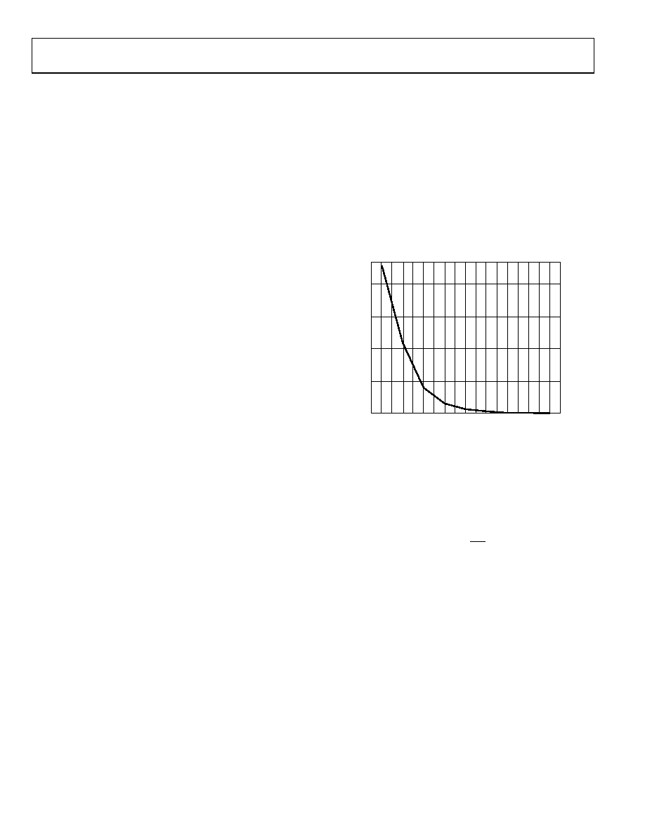
based on activation energy of 0.6 eV, derates with TJ, as shown
150
300
450
600
30
40
55
70
85
100
125
135
150
RE
T
E
NT
IO
N
(
Y
ears)
0
JUNCTION TEMPERATURE (°C)
07079-
016
Figure 22. Flash/EE Memory Data Retention
PROGRAMMING
The 30 kB of Flash/EE memory can be programmed in-circuit,
using the serial download mode or the provided JTAG mode.
Serial Downloading (In-Circuit Programming)
The ADuC706x facilitates code download via the standard
UART serial port. The parts enter serial download mode after a
reset or power cycle if the NTRST/BM pin is pulled low
through an external 1 k resistor. When in serial download
mode, the user can download code to the full 30 kB of Flash/EE
memory while the device is in-circuit in its target application
hardware. An executable PC serial download is provided as part
of the development system for serial downloading via the UART.
When the ADuC706x enters download mode, the user should
be aware that the internal watchdog is enabled with a time-out
period of 2 minutes. If the flash erase/write sequence is not
completed in this period, a reset occurs.
JTAG Access
The JTAG protocol uses the on-chip JTAG interface to facilitate
code download and debug.
相关PDF资料 |
PDF描述 |
|---|---|
| VI-B2L-IW-F4 | CONVERTER MOD DC/DC 28V 100W |
| ATMEGA8535L-8JU | MCU AVR 8K ISP FLASH MEM 44-PLCC |
| VI-B2L-IW-F3 | CONVERTER MOD DC/DC 28V 100W |
| ATMEGA8535L-8PU | IC AVR MCU 8K 8MHZ 3V 40DIP |
| VI-B2L-IW-F2 | CONVERTER MOD DC/DC 28V 100W |
相关代理商/技术参数 |
参数描述 |
|---|---|
| ADUC70SMARTLINKRL7 | 制造商:Analog Devices 功能描述: |
| ADUC70TEL | 制造商:Analog Devices 功能描述:FLASH ARM +5-CH 12BIT ADC - Trays |
| ADUC70TEL-RL7 | 制造商:Analog Devices 功能描述: |
| ADUC7120BBCZ | 制造商:Analog Devices 功能描述:- Rail/Tube |
| ADUC7120BBCZ-RL | 制造商:Analog Devices 功能描述:- Tape and Reel |
发布紧急采购,3分钟左右您将得到回复。