- 您现在的位置:买卖IC网 > PDF目录11210 > ADUC7061BCPZ32-RL (Analog Devices Inc)IC MCU 16/32BIT 32KB 32LFCSP PDF资料下载
参数资料
| 型号: | ADUC7061BCPZ32-RL |
| 厂商: | Analog Devices Inc |
| 文件页数: | 4/108页 |
| 文件大小: | 0K |
| 描述: | IC MCU 16/32BIT 32KB 32LFCSP |
| 产品变化通告: | ADuC7060/1 Idd Specification Change 01/Feb/2010 |
| 设计资源: | USB Based Temperature Monitor Using ADuC7061 and an External RTD (CN0075) 4 mA-to-20 mA Loop-Powered Temperature Monitor Using ADuC7060/1 (CN0145) |
| 标准包装: | 5,000 |
| 系列: | MicroConverter® ADuC7xxx |
| 核心处理器: | ARM7 |
| 芯体尺寸: | 16/32-位 |
| 速度: | 10MHz |
| 连通性: | I²C,SPI,UART/USART |
| 外围设备: | POR,PWM,温度传感器,WDT |
| 输入/输出数: | 8 |
| 程序存储器容量: | 32KB(16K x 16) |
| 程序存储器类型: | 闪存 |
| RAM 容量: | 1K x 32 |
| 电压 - 电源 (Vcc/Vdd): | 2.375 V ~ 2.625 V |
| 数据转换器: | A/D 5x24b,8x24b,D/A 1x14b |
| 振荡器型: | 内部 |
| 工作温度: | -40°C ~ 125°C |
| 封装/外壳: | 32-VFQFN 裸露焊盘,CSP |
| 包装: | 带卷 (TR) |
第1页第2页第3页当前第4页第5页第6页第7页第8页第9页第10页第11页第12页第13页第14页第15页第16页第17页第18页第19页第20页第21页第22页第23页第24页第25页第26页第27页第28页第29页第30页第31页第32页第33页第34页第35页第36页第37页第38页第39页第40页第41页第42页第43页第44页第45页第46页第47页第48页第49页第50页第51页第52页第53页第54页第55页第56页第57页第58页第59页第60页第61页第62页第63页第64页第65页第66页第67页第68页第69页第70页第71页第72页第73页第74页第75页第76页第77页第78页第79页第80页第81页第82页第83页第84页第85页第86页第87页第88页第89页第90页第91页第92页第93页第94页第95页第96页第97页第98页第99页第100页第101页第102页第103页第104页第105页第106页第107页第108页
Data Sheet
ADuC7060/ADuC7061
Rev. D | Page 101 of 108
GENERAL-PURPOSE I/O
The ADuC706x features up to 16 general-purpose bidirectional
input/output (GPIO) pins. In general, many of the GPIO pins have
multiple functions that are configurable by user code. By default,
the GPIO pins are configured in GPIO mode. All GPIO pins have
an internal pull-up resistor with a drive capability of 1.6 mA.
All I/O pins are 3.3 V tolerant, meaning that the GPIOs support
an input voltage of 3.3 V.
When the ADuC706x enters power-saving mode, the GPIO
pins retain their state.
The GPIO pins are grouped into three port buses.
Table 110 lists all the GPIO pins and their alternative functions.
A GPIO pin alternative function can be selected by writing to
the correct bits of the GPxCON register.
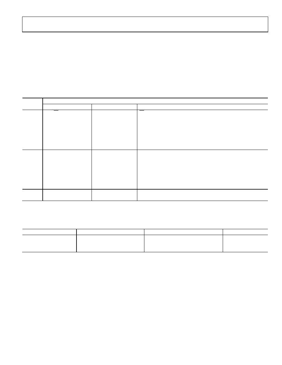
Table 110. GPIO Multifunction Pin Descriptions
Port
Configuration via GPxCON Including GP0CON0
Pin Mnemonic
00
01
0
P0.0/SS
GPIO
SS (SPI slave select).
P0.1/SCLK/SCL
GPIO
SCLK/SCL (serial clock/SPI clock).
P0.2/MISO
GPIO
MISO (SPI—master in/slave out).
P0.3/MOSI/SDA
GPIO
MOSI (SPI—master out/slave in).
P0.4/IRQ0/PWM1
GPIO/IRQ0
PWM1 (PWM Output 1).
P0.5/CTS
GPIO
CTS. UART clear to send pin.
P0.6/RTS
GPIO
RTS. UART request to send pin.
1
P1.0/IRQ1/SIN/T0
GPIO/IRQ1
SIN (serial input).
P1.1/SOUT
GPIO
SOUT (serial output).
P1.2/SYNC
GPIO
PWM sync (PWM sync input pin).
P1.3/TRIP
GPIO
PWM trip (PWM trip input pin).
P1.4/PWM2
GPIO
PWM2 (PWM Output 2).
P1.5/PWM3
GPIO
PWM3 (PWM Output 3).
P1.6/PWM4
GPIO
PWM4 (PWM Output 4).
2
P2.0/IRQ2/PWM0/EXTCLK
GPIO/IRQ2/EXTCLK
PWM0 (PWM Output 0).
P2.1/IRQ3/PWM5
GPIO/IRQ3
PWM5 (PWM Output 5).
GPxCON REGISTERS
GPxCON are the Port x (where x is 0, 1, or 2) control registers, which select the function of each pin of Port x as described in Table 112.
Table 111. GPxCON Registers
Name
Address
Default Value
Access
GP0CON0
0xFFFF0D00
0x00000000
R/W
GP1CON
0xFFFF0D04
0x00000000
R/W
GP2CON
0xFFFF0D08
0x00000000
R/W
相关PDF资料 |
PDF描述 |
|---|---|
| VI-B2L-IW-F4 | CONVERTER MOD DC/DC 28V 100W |
| ATMEGA8535L-8JU | MCU AVR 8K ISP FLASH MEM 44-PLCC |
| VI-B2L-IW-F3 | CONVERTER MOD DC/DC 28V 100W |
| ATMEGA8535L-8PU | IC AVR MCU 8K 8MHZ 3V 40DIP |
| VI-B2L-IW-F2 | CONVERTER MOD DC/DC 28V 100W |
相关代理商/技术参数 |
参数描述 |
|---|---|
| ADUC70SMARTLINKRL7 | 制造商:Analog Devices 功能描述: |
| ADUC70TEL | 制造商:Analog Devices 功能描述:FLASH ARM +5-CH 12BIT ADC - Trays |
| ADUC70TEL-RL7 | 制造商:Analog Devices 功能描述: |
| ADUC7120BBCZ | 制造商:Analog Devices 功能描述:- Rail/Tube |
| ADUC7120BBCZ-RL | 制造商:Analog Devices 功能描述:- Tape and Reel |
发布紧急采购,3分钟左右您将得到回复。