- 您现在的位置:买卖IC网 > PDF目录378053 > PM4354 (PMC-Sierra, Inc.) Ultraframer DS3/E3/DS2/E2/DS1/E1/DS0 PDF资料下载
参数资料
| 型号: | PM4354 |
| 厂商: | PMC-Sierra, Inc. |
| 元件分类: | 通信及网络 |
| 英文描述: | Ultraframer DS3/E3/DS2/E2/DS1/E1/DS0 |
| 中文描述: | Ultraframer DS3/E3/DS2/E2/DS1/E1/DS0 |
| 文件页数: | 435/463页 |
| 文件大小: | 3726K |
| 代理商: | PM4354 |
第1页第2页第3页第4页第5页第6页第7页第8页第9页第10页第11页第12页第13页第14页第15页第16页第17页第18页第19页第20页第21页第22页第23页第24页第25页第26页第27页第28页第29页第30页第31页第32页第33页第34页第35页第36页第37页第38页第39页第40页第41页第42页第43页第44页第45页第46页第47页第48页第49页第50页第51页第52页第53页第54页第55页第56页第57页第58页第59页第60页第61页第62页第63页第64页第65页第66页第67页第68页第69页第70页第71页第72页第73页第74页第75页第76页第77页第78页第79页第80页第81页第82页第83页第84页第85页第86页第87页第88页第89页第90页第91页第92页第93页第94页第95页第96页第97页第98页第99页第100页第101页第102页第103页第104页第105页第106页第107页第108页第109页第110页第111页第112页第113页第114页第115页第116页第117页第118页第119页第120页第121页第122页第123页第124页第125页第126页第127页第128页第129页第130页第131页第132页第133页第134页第135页第136页第137页第138页第139页第140页第141页第142页第143页第144页第145页第146页第147页第148页第149页第150页第151页第152页第153页第154页第155页第156页第157页第158页第159页第160页第161页第162页第163页第164页第165页第166页第167页第168页第169页第170页第171页第172页第173页第174页第175页第176页第177页第178页第179页第180页第181页第182页第183页第184页第185页第186页第187页第188页第189页第190页第191页第192页第193页第194页第195页第196页第197页第198页第199页第200页第201页第202页第203页第204页第205页第206页第207页第208页第209页第210页第211页第212页第213页第214页第215页第216页第217页第218页第219页第220页第221页第222页第223页第224页第225页第226页第227页第228页第229页第230页第231页第232页第233页第234页第235页第236页第237页第238页第239页第240页第241页第242页第243页第244页第245页第246页第247页第248页第249页第250页第251页第252页第253页第254页第255页第256页第257页第258页第259页第260页第261页第262页第263页第264页第265页第266页第267页第268页第269页第270页第271页第272页第273页第274页第275页第276页第277页第278页第279页第280页第281页第282页第283页第284页第285页第286页第287页第288页第289页第290页第291页第292页第293页第294页第295页第296页第297页第298页第299页第300页第301页第302页第303页第304页第305页第306页第307页第308页第309页第310页第311页第312页第313页第314页第315页第316页第317页第318页第319页第320页第321页第322页第323页第324页第325页第326页第327页第328页第329页第330页第331页第332页第333页第334页第335页第336页第337页第338页第339页第340页第341页第342页第343页第344页第345页第346页第347页第348页第349页第350页第351页第352页第353页第354页第355页第356页第357页第358页第359页第360页第361页第362页第363页第364页第365页第366页第367页第368页第369页第370页第371页第372页第373页第374页第375页第376页第377页第378页第379页第380页第381页第382页第383页第384页第385页第386页第387页第388页第389页第390页第391页第392页第393页第394页第395页第396页第397页第398页第399页第400页第401页第402页第403页第404页第405页第406页第407页第408页第409页第410页第411页第412页第413页第414页第415页第416页第417页第418页第419页第420页第421页第422页第423页第424页第425页第426页第427页第428页第429页第430页第431页第432页第433页第434页当前第435页第436页第437页第438页第439页第440页第441页第442页第443页第444页第445页第446页第447页第448页第449页第450页第451页第452页第453页第454页第455页第456页第457页第458页第459页第460页第461页第462页第463页
RELEASED
PM4354 COMET-QUAD
DATASHEET
PMC-1990315
ISSUE 6
FOUR CHANNEL COMBINED E1/T1/J1
TRANSCEIVER / FRAMER
PROPRIETARY AND CONFIDENTIAL TO PMC-SIERRA, INC. AND FOR ITS CUSTOMERS’ INTERNAL USE
420
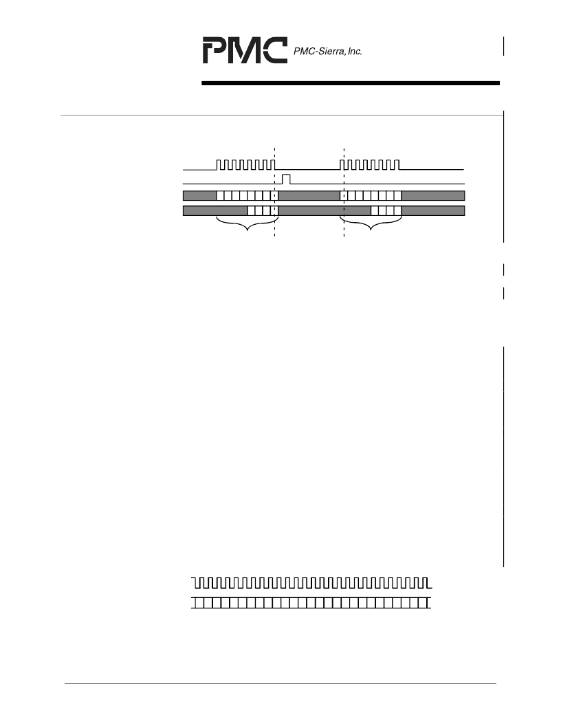
Figure 68: - E1 Transmit Clock Master: Nx64Kbit/s Mode (DE=0, FE=0)
Timeslot 31
Timeslot 1
1 2
4
3
5 6 7 8
1 2
4
3
5 6 7 8
A B C D
A B C D
BTFP[x]
BTPCM[x]
BTSIG[x]
BTCLK[x]
The BTIF Configuration register is programmed to select Nx64Kbit/s mode. The TPSC PCM Data
Control bytes are programmed to insert the desired channels. In Figure 65 and Figure 67, the
PCM Data Control bytes for T1 channels 1 and 24 are configured to insert BTPCM[x] data into
these channels. In Figure 66 and Figure 68, the PCM Data Control bytes for E1 channels 1 and
31 are configured to insert BTPCM[x] data into these channels. BTCLK[x] is gapped so that it is
only active for those channels with the associated IDLE_CHAN bit cleared (logic 0). The
remaining channels (with IDLE_CHAN set) contain the per-channel idle code as defined in the
associated Idle Code byte.
In Figure 65 and Figure 66, the BTIF’s DE bit is logic 1, indicating that BTPCM[x] and BTSIG[x]
are sampled on the rising edge of BTCLK[x]; the BTIF’s FE bit is logic 0, indicating that BTFP[x]
updates on the falling edge of BTCLK[x]. Since BTFP[x] is an output and DE and FE have
opposite values, BTFP[x] updates three clock edges before where the first bit of the frame would
be sampled (assuming the clock were not gapped). In Figure 67 and Figure 68, the BTIF’s DE bit
is logic 0, indicating that BTPCM[x] and BTSIG[x] are sampled on the falling edge of BTCLK[x];
the BTIF’s FE bit is logic 0, indicating that the BTFP[x] output updates on the falling edge of
BTCLK[x].
The level of the clock gap is determined by the BTIF’s DE bit. If DE is logic 0, the clock gap is
logic 0; if DE is logic 1, the clock gap is logic 1.
If DE and FE were both logic 1, the functional timing is as described in Figure 65 and Figure 66
but with BTFP[x] updating three clock edges later (assuming the clock were not gapped). If DE
were logic 0 and FE logic 1, then the functional timing is as described in Figure 67 and Figure 68
but with BTFP[x] updating three clock edges earlier (assuming the clock were not gapped).
Figure 69: - T1/E1 Transmit Clock Master : Clear Channel Mode
BTCLK[x]
BTPCM[x]
1 2
4
3
5 6 7 8 1 2
4
3
5 6 7 8 1 2
4
3
5 6 7 8 1 2
8
The Backplane Transmit Interface is configured for the Clock Master: Clear Channel mode by
programming the CMODE bit of the BTIF Configuration register to logic 0 and the FDIS bit of the
相关PDF资料 |
PDF描述 |
|---|---|
| PM4388 | Ultraframer DS3/E3/DS2/E2/DS1/E1/DS0 |
| PM4388-NI | Ultraframer DS3/E3/DS2/E2/DS1/E1/DS0 |
| PM4388-RI | Ultraframer DS3/E3/DS2/E2/DS1/E1/DS0 |
| PM4541 | T1XC EVALUATION DAUGHTER BOARD |
| PM49FL002 | 2 Mbit / 4 Mbit 3.3 Volt-only Firmware Hub/LPC Flash Memory |
相关代理商/技术参数 |
参数描述 |
|---|---|
| PM4354-NI | 制造商:PMC-Sierra 功能描述: |
| PM4354-PI | 制造商:PMC 制造商全称:PMC 功能描述:FOUR CHANNEL COMBINED E1/T1/J1 TRANSCEIVER/FRAMER |
| PM43-560K | 功能描述:固定电感器 56uH 10% RoHS:否 制造商:AVX 电感:10 uH 容差:20 % 最大直流电流:1 A 最大直流电阻:0.075 Ohms 工作温度范围:- 40 C to + 85 C 自谐振频率:38 MHz Q 最小值:40 尺寸:4.45 mm W x 6.6 mm L x 2.92 mm H 屏蔽:Shielded 端接类型:SMD/SMT 封装 / 箱体:6.6 mm x 4.45 mm |
| PM43-560K-RC | 功能描述:固定电感器 56uH 10% RoHS:否 制造商:AVX 电感:10 uH 容差:20 % 最大直流电流:1 A 最大直流电阻:0.075 Ohms 工作温度范围:- 40 C to + 85 C 自谐振频率:38 MHz Q 最小值:40 尺寸:4.45 mm W x 6.6 mm L x 2.92 mm H 屏蔽:Shielded 端接类型:SMD/SMT 封装 / 箱体:6.6 mm x 4.45 mm |
发布紧急采购,3分钟左右您将得到回复。