- 您现在的位置:买卖IC网 > PDF目录378053 > PM4354 (PMC-Sierra, Inc.) Ultraframer DS3/E3/DS2/E2/DS1/E1/DS0 PDF资料下载
参数资料
| 型号: | PM4354 |
| 厂商: | PMC-Sierra, Inc. |
| 元件分类: | 通信及网络 |
| 英文描述: | Ultraframer DS3/E3/DS2/E2/DS1/E1/DS0 |
| 中文描述: | Ultraframer DS3/E3/DS2/E2/DS1/E1/DS0 |
| 文件页数: | 438/463页 |
| 文件大小: | 3726K |
| 代理商: | PM4354 |
第1页第2页第3页第4页第5页第6页第7页第8页第9页第10页第11页第12页第13页第14页第15页第16页第17页第18页第19页第20页第21页第22页第23页第24页第25页第26页第27页第28页第29页第30页第31页第32页第33页第34页第35页第36页第37页第38页第39页第40页第41页第42页第43页第44页第45页第46页第47页第48页第49页第50页第51页第52页第53页第54页第55页第56页第57页第58页第59页第60页第61页第62页第63页第64页第65页第66页第67页第68页第69页第70页第71页第72页第73页第74页第75页第76页第77页第78页第79页第80页第81页第82页第83页第84页第85页第86页第87页第88页第89页第90页第91页第92页第93页第94页第95页第96页第97页第98页第99页第100页第101页第102页第103页第104页第105页第106页第107页第108页第109页第110页第111页第112页第113页第114页第115页第116页第117页第118页第119页第120页第121页第122页第123页第124页第125页第126页第127页第128页第129页第130页第131页第132页第133页第134页第135页第136页第137页第138页第139页第140页第141页第142页第143页第144页第145页第146页第147页第148页第149页第150页第151页第152页第153页第154页第155页第156页第157页第158页第159页第160页第161页第162页第163页第164页第165页第166页第167页第168页第169页第170页第171页第172页第173页第174页第175页第176页第177页第178页第179页第180页第181页第182页第183页第184页第185页第186页第187页第188页第189页第190页第191页第192页第193页第194页第195页第196页第197页第198页第199页第200页第201页第202页第203页第204页第205页第206页第207页第208页第209页第210页第211页第212页第213页第214页第215页第216页第217页第218页第219页第220页第221页第222页第223页第224页第225页第226页第227页第228页第229页第230页第231页第232页第233页第234页第235页第236页第237页第238页第239页第240页第241页第242页第243页第244页第245页第246页第247页第248页第249页第250页第251页第252页第253页第254页第255页第256页第257页第258页第259页第260页第261页第262页第263页第264页第265页第266页第267页第268页第269页第270页第271页第272页第273页第274页第275页第276页第277页第278页第279页第280页第281页第282页第283页第284页第285页第286页第287页第288页第289页第290页第291页第292页第293页第294页第295页第296页第297页第298页第299页第300页第301页第302页第303页第304页第305页第306页第307页第308页第309页第310页第311页第312页第313页第314页第315页第316页第317页第318页第319页第320页第321页第322页第323页第324页第325页第326页第327页第328页第329页第330页第331页第332页第333页第334页第335页第336页第337页第338页第339页第340页第341页第342页第343页第344页第345页第346页第347页第348页第349页第350页第351页第352页第353页第354页第355页第356页第357页第358页第359页第360页第361页第362页第363页第364页第365页第366页第367页第368页第369页第370页第371页第372页第373页第374页第375页第376页第377页第378页第379页第380页第381页第382页第383页第384页第385页第386页第387页第388页第389页第390页第391页第392页第393页第394页第395页第396页第397页第398页第399页第400页第401页第402页第403页第404页第405页第406页第407页第408页第409页第410页第411页第412页第413页第414页第415页第416页第417页第418页第419页第420页第421页第422页第423页第424页第425页第426页第427页第428页第429页第430页第431页第432页第433页第434页第435页第436页第437页当前第438页第439页第440页第441页第442页第443页第444页第445页第446页第447页第448页第449页第450页第451页第452页第453页第454页第455页第456页第457页第458页第459页第460页第461页第462页第463页
RELEASED
PM4354 COMET-QUAD
DATASHEET
PMC-1990315
ISSUE 6
FOUR CHANNEL COMBINED E1/T1/J1
TRANSCEIVER / FRAMER
PROPRIETARY AND CONFIDENTIAL TO PMC-SIERRA, INC. AND FOR ITS CUSTOMERS’ INTERNAL USE
423
BTPCM[x] is sampled on the falling edge of BTCLK[x], and the functional timing is described by
Figure 73 with the BTCLK[x] signal inverted.
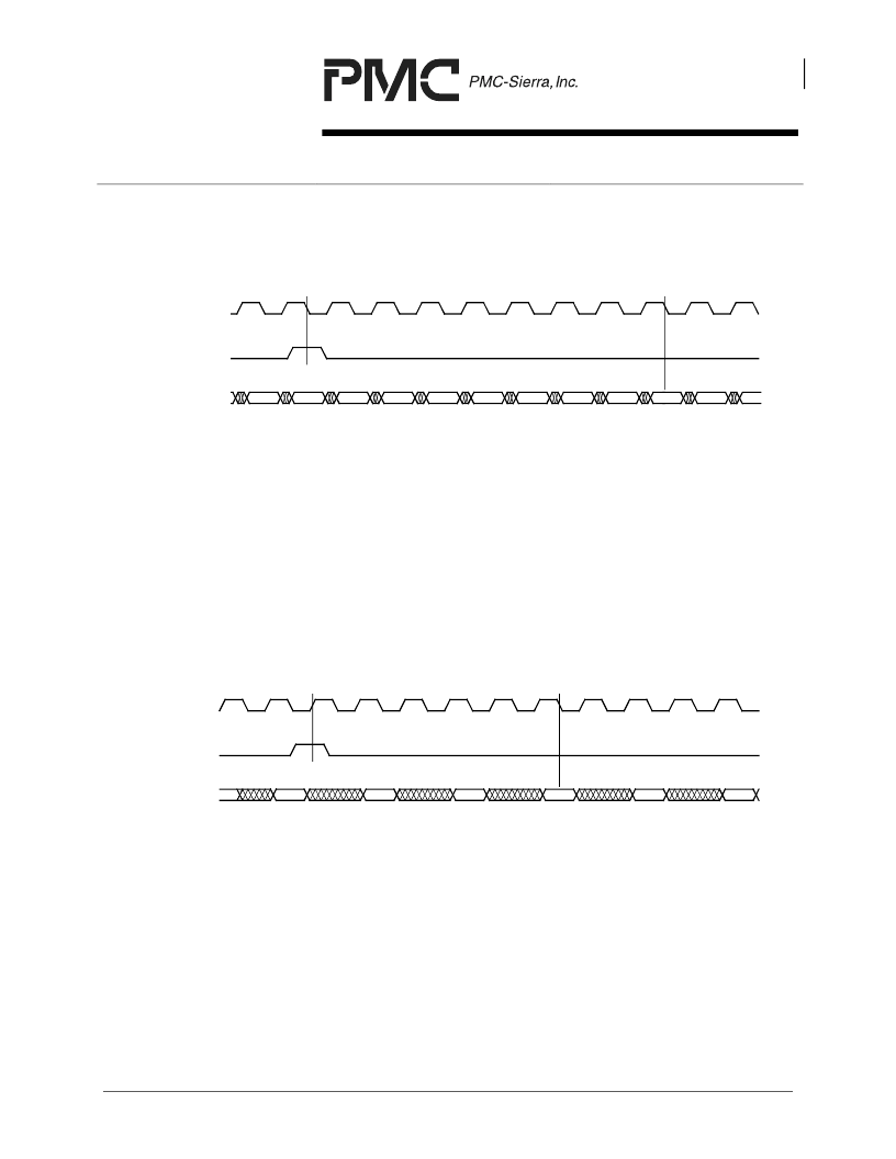
Figure 74: - Concentration Highway Interface Timing, Example1
bit 0 TS 0
bit 1 TS 0
bit 2 TS 0
bit 3 TS 0
bit 4 TS 0
bit 5 TS 0
bit 6 TS 0
bit 7 TS 0
bit 0 TS 1
bit 7 TS 31
bit 2 TS 1
bit 1 TS 1
BTCLK[x]
BTFP[x]
BTPCM[x]
1
2
3
4
5
6
7
8
9
10
11
12
CER = 16
13
14
15
16
17
18
Concentration Highway Interface (CHI) timing is configured by setting the BOFF_EN bit of the
BTIF Configuration register to logic 1. In Figure 74, the BTIF’s DE and FE register bits are set to
logic 0 so that BTPCM[x], BTSIG[x], and BTFP[x] are sampled on the falling edge of BTCLK[x].
CMS is set to logic 0 so that the clock rate is equal to the data rate. BOFF[2:0] is set to ‘b110 so
that the receive clock edge (CER) is equal to 16 (as determined by the table in the BTIF Bit Offset
register description of BOFF[2:0]) and BTPCM[x] (and BTSIG[x]) is sampled 16 clock edges after
BTFP[x] is sampled. TSOFF[6:0] is set to ‘b0000000 so that there is no timeslot offset. In the
above example, if TSOFF[6:0] were set to ‘b0011111, then BTPCM[x] would be sampled an
additional 31 timeslots later, exactly one E1 frame after BTFP[x] was sampled as logic 1. In the
above example, if TSOFF[6:0] were set to ‘b0010111, then BTPCM[x] would be sampled an
additional 23 timeslots later, exactly one T1 frame after BTFP[x] was sampled as logic 1.
Figure 75: - Concentration Highway Interface Timing, Example 2
BTCLK[x]
BTPCM[x]
bit 0 TS 0
bit 1 TS 0
bit 2 TS 0
1
2
3
4
5
6
7
8
9
10
11
12
bit 7 TS 31
bit 6 TS 31
bit 5 TS 31
CER = 11
BTFP[x]
Concentration Highway Interface (CHI) timing is configured by setting the BOFF_EN bit of the
BTIF Configuration register to logic 1. In Figure 75, the BTIF’s FE register bit is set to logic 1 so
that BTFP[x] is sampled on the rising edge of BTCLK[x]. The DE register bit is set to logic 0 so
that BTPCM[x] is sampled on the falling edge of BTCLK[x]. CMS is set to logic 1 so that the clock
rate is equal to two times the data rate. BOFF[2:0] is set to ‘b001 so that the receive clock edge
(CER) is equal to 11 (as determined by the table in the BTIF Bit Offset register description of
BOFF[2:0]) and BTPCM[x] is sampled 11 clock edges after BTFP[x] is sampled. TSOFF[6:0] is set
to ‘b0000000 so that there is no timeslot offset.
相关PDF资料 |
PDF描述 |
|---|---|
| PM4388 | Ultraframer DS3/E3/DS2/E2/DS1/E1/DS0 |
| PM4388-NI | Ultraframer DS3/E3/DS2/E2/DS1/E1/DS0 |
| PM4388-RI | Ultraframer DS3/E3/DS2/E2/DS1/E1/DS0 |
| PM4541 | T1XC EVALUATION DAUGHTER BOARD |
| PM49FL002 | 2 Mbit / 4 Mbit 3.3 Volt-only Firmware Hub/LPC Flash Memory |
相关代理商/技术参数 |
参数描述 |
|---|---|
| PM4354-NI | 制造商:PMC-Sierra 功能描述: |
| PM4354-PI | 制造商:PMC 制造商全称:PMC 功能描述:FOUR CHANNEL COMBINED E1/T1/J1 TRANSCEIVER/FRAMER |
| PM43-560K | 功能描述:固定电感器 56uH 10% RoHS:否 制造商:AVX 电感:10 uH 容差:20 % 最大直流电流:1 A 最大直流电阻:0.075 Ohms 工作温度范围:- 40 C to + 85 C 自谐振频率:38 MHz Q 最小值:40 尺寸:4.45 mm W x 6.6 mm L x 2.92 mm H 屏蔽:Shielded 端接类型:SMD/SMT 封装 / 箱体:6.6 mm x 4.45 mm |
| PM43-560K-RC | 功能描述:固定电感器 56uH 10% RoHS:否 制造商:AVX 电感:10 uH 容差:20 % 最大直流电流:1 A 最大直流电阻:0.075 Ohms 工作温度范围:- 40 C to + 85 C 自谐振频率:38 MHz Q 最小值:40 尺寸:4.45 mm W x 6.6 mm L x 2.92 mm H 屏蔽:Shielded 端接类型:SMD/SMT 封装 / 箱体:6.6 mm x 4.45 mm |
发布紧急采购,3分钟左右您将得到回复。