- 您现在的位置:买卖IC网 > PDF目录17102 > ORSO42G5-EV (Lattice Semiconductor Corporation)BOARD EVAL DEV PLATFORM ORSO42G5 PDF资料下载
参数资料
| 型号: | ORSO42G5-EV |
| 厂商: | Lattice Semiconductor Corporation |
| 文件页数: | 101/153页 |
| 文件大小: | 0K |
| 描述: | BOARD EVAL DEV PLATFORM ORSO42G5 |
| 标准包装: | 1 |
| 系列: | ORCA® 4 系列 |
| 类型: | FPGA |
| 适用于相关产品: | ORSO42G5 |
| 所含物品: | 板,线缆,电源 |
| 其它名称: | ORSO42G5EV |
第1页第2页第3页第4页第5页第6页第7页第8页第9页第10页第11页第12页第13页第14页第15页第16页第17页第18页第19页第20页第21页第22页第23页第24页第25页第26页第27页第28页第29页第30页第31页第32页第33页第34页第35页第36页第37页第38页第39页第40页第41页第42页第43页第44页第45页第46页第47页第48页第49页第50页第51页第52页第53页第54页第55页第56页第57页第58页第59页第60页第61页第62页第63页第64页第65页第66页第67页第68页第69页第70页第71页第72页第73页第74页第75页第76页第77页第78页第79页第80页第81页第82页第83页第84页第85页第86页第87页第88页第89页第90页第91页第92页第93页第94页第95页第96页第97页第98页第99页第100页当前第101页第102页第103页第104页第105页第106页第107页第108页第109页第110页第111页第112页第113页第114页第115页第116页第117页第118页第119页第120页第121页第122页第123页第124页第125页第126页第127页第128页第129页第130页第131页第132页第133页第134页第135页第136页第137页第138页第139页第140页第141页第142页第143页第144页第145页第146页第147页第148页第149页第150页第151页第152页第153页
Lattice Semiconductor
ORCA ORSO42G5 and ORSO82G5 Data Sheet
51
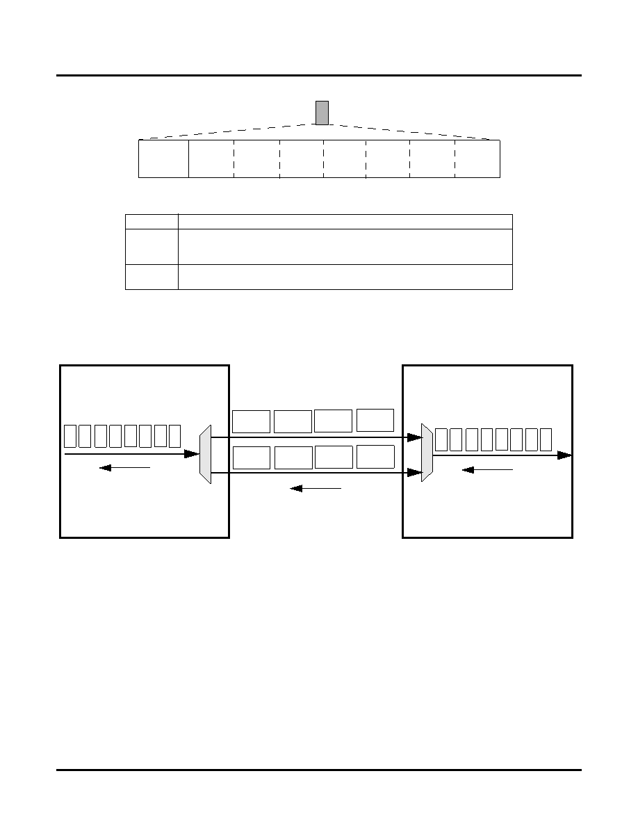
Figure 37. Link Header Byte
Table 10. Link Header Format
In cell mode, multiple SERDES links are used to achieve desired bandwidth. Data are cell-striped in a round-robin
fashion across two or eight links by the transmitter and then re-assembled back into a single cell stream (destrip-
ing) by the receiver. This is shown in Figure 38.
Figure 38. Multi-Link Interface - Two-Link Example
To assist with cell delineation, each link transmitter assigns sequence numbers to cells (LSEQN[6:0] bits in the Link
Header byte) before sending them out on the link. Each link increments its sequence numbers independently as
shown in Figure 38. All links reset their sequence number generator at the beginning of a SONET frame (All links
are synchronized to the start of a frame).
On the receiving side, each receiver uses the sequence numbers to verify the correct cell delineation. Since the
links were synchronized to the start of the SONET frame, all links will have cells with the same sequence number
available at the same time (although deskew needs to happen to properly align the cells). This allows the receiver
to correctly reconstruct the original cell stream.
If an unexpected sequence number is received, the receiver does not use the received value as the basis for the
next expected sequence number. Rather the old expected value is incremented by one, forming the new expected
value. An error ag is sent to the software register interface and the cell will be marked with an error. For example,
assume that the receiver expected to receive a cell with sequence number 27, but received one with sequence
number 37. The cell will be marked with an error. The receiver then expects to receive a cell with sequence number
28.
Location
Field/Description
7
Idle: Idle Cell Indicator
0: User Cell (contains valid data)
1: Idle Cell (no data in the cell payload)
6:0
LSEQ: Link Sequence Number. This value is used when aligning cells from
multiple links when doing link group multiplexing.
LIDLE
LSEQN[6:0]
LINK HEADER BYTE
Time
TRANSMITTER
Time
3
2
1
0
7
6
5
4
CELL STRIPING
0
1
LSEQ = 3
Cell = 7
LSEQ = 2
Cell = 5
LSEQ = 1
Cell = 3
LSEQ = 0
Cell = 1
Time
RECEIVER
3
2
1
0
7
6
5
4
CELL DE-STRIPING
0
1
LSEQ = 3
Cell = 6
LSEQ = 2
Cell = 4
LSEQ = 1
Cell = 2
LSEQ = 0
Cell = 0
相关PDF资料 |
PDF描述 |
|---|---|
| EEM22DTAT-S189 | CONN EDGECARD 44POS R/A .156 SLD |
| ECC20DRES | CONN EDGECARD 40POS .100 EYELET |
| AT-S-26-4/4/W-25-R | MOD CORD STANDARD 4-4 WHITE 25' |
| EEC40DREI | CONN EDGECARD 80POS .100 EYELET |
| 0210490869 | CABLE JUMPER 1.25MM .203M 17POS |
相关代理商/技术参数 |
参数描述 |
|---|---|
| ORSO82G5 | 制造商:LATTICE 制造商全称:Lattice Semiconductor 功能描述:0.6 to 2.7 Gbps SONET Backplane Interface FPSCs |
| ORSO82G5-1BM680C | 功能描述:FPGA - 现场可编程门阵列 10368 LUT 372 I/O RoHS:否 制造商:Altera Corporation 系列:Cyclone V E 栅极数量: 逻辑块数量:943 内嵌式块RAM - EBR:1956 kbit 输入/输出端数量:128 最大工作频率:800 MHz 工作电源电压:1.1 V 最大工作温度:+ 70 C 安装风格:SMD/SMT 封装 / 箱体:FBGA-256 |
| ORSO82G5-1BM680I | 功能描述:FPGA - 现场可编程门阵列 10368 LUT 372 I/O RoHS:否 制造商:Altera Corporation 系列:Cyclone V E 栅极数量: 逻辑块数量:943 内嵌式块RAM - EBR:1956 kbit 输入/输出端数量:128 最大工作频率:800 MHz 工作电源电压:1.1 V 最大工作温度:+ 70 C 安装风格:SMD/SMT 封装 / 箱体:FBGA-256 |
| ORSO82G5-1F680C | 功能描述:FPGA - 现场可编程门阵列 ORCA FPSC 2.7GBITS/s BP XCVR 643K RoHS:否 制造商:Altera Corporation 系列:Cyclone V E 栅极数量: 逻辑块数量:943 内嵌式块RAM - EBR:1956 kbit 输入/输出端数量:128 最大工作频率:800 MHz 工作电源电压:1.1 V 最大工作温度:+ 70 C 安装风格:SMD/SMT 封装 / 箱体:FBGA-256 |
| ORSO82G5-1F680I | 功能描述:FPGA - 现场可编程门阵列 ORCA FPSC 2.7Gbits/s BP XCVR 643K RoHS:否 制造商:Altera Corporation 系列:Cyclone V E 栅极数量: 逻辑块数量:943 内嵌式块RAM - EBR:1956 kbit 输入/输出端数量:128 最大工作频率:800 MHz 工作电源电压:1.1 V 最大工作温度:+ 70 C 安装风格:SMD/SMT 封装 / 箱体:FBGA-256 |
发布紧急采购,3分钟左右您将得到回复。