- 您现在的位置:买卖IC网 > PDF目录17102 > ORSO42G5-EV (Lattice Semiconductor Corporation)BOARD EVAL DEV PLATFORM ORSO42G5 PDF资料下载
参数资料
| 型号: | ORSO42G5-EV |
| 厂商: | Lattice Semiconductor Corporation |
| 文件页数: | 128/153页 |
| 文件大小: | 0K |
| 描述: | BOARD EVAL DEV PLATFORM ORSO42G5 |
| 标准包装: | 1 |
| 系列: | ORCA® 4 系列 |
| 类型: | FPGA |
| 适用于相关产品: | ORSO42G5 |
| 所含物品: | 板,线缆,电源 |
| 其它名称: | ORSO42G5EV |
第1页第2页第3页第4页第5页第6页第7页第8页第9页第10页第11页第12页第13页第14页第15页第16页第17页第18页第19页第20页第21页第22页第23页第24页第25页第26页第27页第28页第29页第30页第31页第32页第33页第34页第35页第36页第37页第38页第39页第40页第41页第42页第43页第44页第45页第46页第47页第48页第49页第50页第51页第52页第53页第54页第55页第56页第57页第58页第59页第60页第61页第62页第63页第64页第65页第66页第67页第68页第69页第70页第71页第72页第73页第74页第75页第76页第77页第78页第79页第80页第81页第82页第83页第84页第85页第86页第87页第88页第89页第90页第91页第92页第93页第94页第95页第96页第97页第98页第99页第100页第101页第102页第103页第104页第105页第106页第107页第108页第109页第110页第111页第112页第113页第114页第115页第116页第117页第118页第119页第120页第121页第122页第123页第124页第125页第126页第127页当前第128页第129页第130页第131页第132页第133页第134页第135页第136页第137页第138页第139页第140页第141页第142页第143页第144页第145页第146页第147页第148页第149页第150页第151页第152页第153页
Lattice Semiconductor
ORCA ORSO42G5 and ORSO82G5 Data Sheet
76
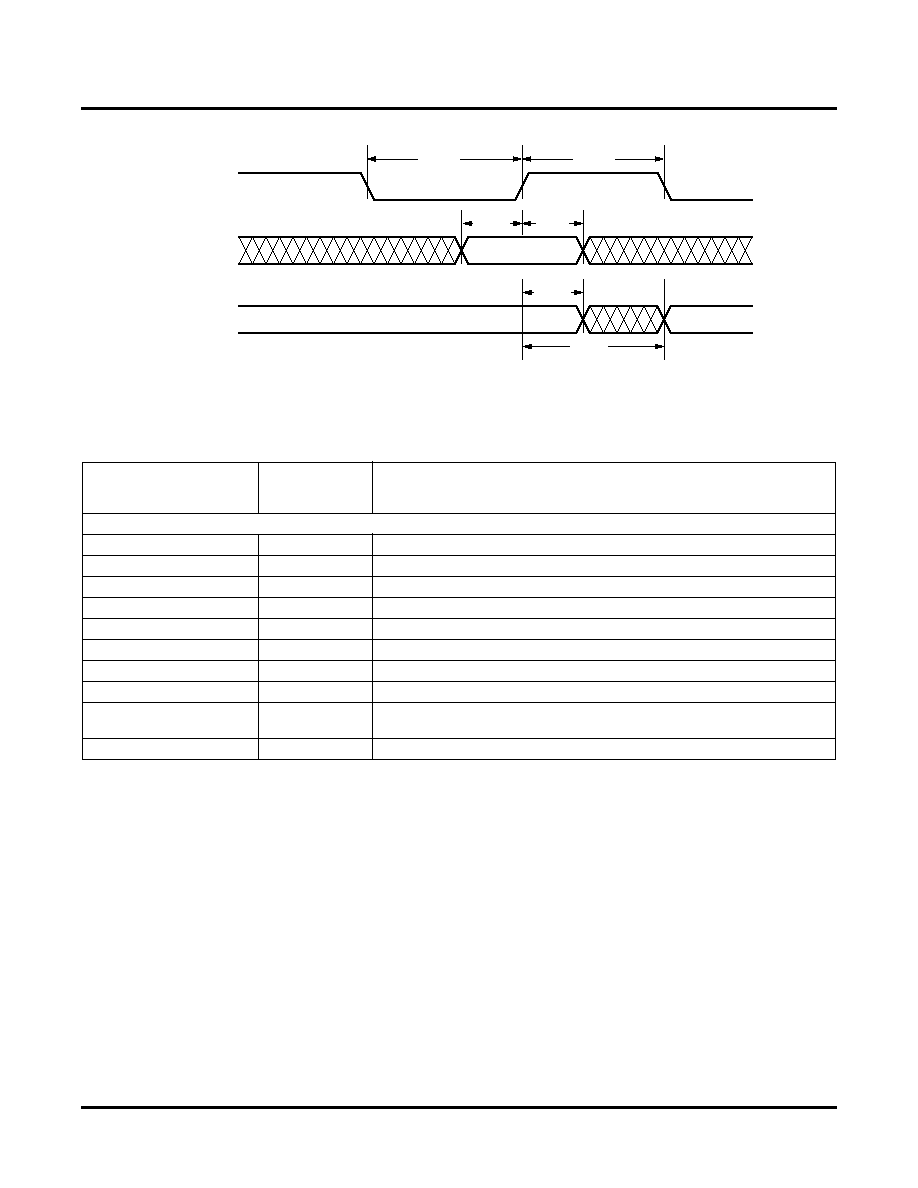
Figure 50. Minimum Timing Specs for Memory Blocks-Read Cycle (-1 Speed Grade)
Table 19 summarizes the Embedded Memory Signals at the Core/FPGA interface. In the table, an input refers to a
signal owing into the embedded core and an output refers to a signal owing out of the embedded core.
Table 19. Embedded Memory Core/FPGA Interface Signal Description
Register Maps
The memory map for the ORSO42G5 and ORSO82G5 core is only part of the full memory map of the ORSO42G5
and ORSO82G5 devices. The ORSO42G5 and ORSO82G5 are ORCA Series 4 based devices and thus use the
system bus as a communication bridge. The ORSO42G5 and ORSO82G5 core register map contained in this data
sheet only covers the embedded ASIC core of the device, not the entire device. The system bus itself, and the
generic FPGA memory map, are fully documented in the MPI/System Bus Application Note. As part of the system
bus, the embedded ASIC core of an FPSC is located at address offset 0x30000. The ORSO42G5 and ORSO82G5
embedded core is an eight-bit slave interface on the Series 4 system bus. The ORSO42G5 and ORSO82G5 core
registers are clocked by the system bus main clock.
Each ORCA device contains a device ID. This device ID is unique to each ORCA device and can be used for device
identication and assist in the system debugging. The device ID is located at absolute address 0x0-0x3. The
ORSO42G5 and ORCA82G5 device IDs are 0xDC012282. More information on the device ID and other Series 4
generic registers can be found in technical note TN1017, ORCA Series 4 MPI/System Bus.
If a clock is not provided to the reference clock, the registers will fail to operate.
FPGA/Embedded Core
Interface Signal Name]
Input (I) to
or Output (O)
from Core
Signal Description
Memory Slice Interface Signals
D_[A:B][35:0]
I
Data in – memory slice [A:B]
CKW_[A:B]
I
Write clock – memory slice [A:B].
CSWA_[A:B]
I
Write chip select for SRAM A – memory slice [A:B].
CSWB_[A:B]
I
Write chip select for SRAM B – memory slice [A:B].
AW_[A:B][10:0]
I
Write address – memory slice [A:B].
BYTEWN_[A:B][3:0]
I
Write control pins for byte-at-a-time write-memory slice [A:B].
Q_[A:B][35:0]
O
Data out – memory slice [A:B].
CKR_[A:B]
I
Read clock – memory slice [A:B].
CSR_[A:B]
I
Read chip select – memory slice [A:B]. CSR_[A:B]= 0 selects SRAM A.
CSR_[A:B]= 1 selects SRAM B.
AR_[A:B][10:0]
I
Read address – memory slice [A:B].
CKR
AR[10:0],
CSR
Q[35:0]
1.5 ns
4.5 ns
0.5 ns
2.0 ns
0 ns
相关PDF资料 |
PDF描述 |
|---|---|
| EEM22DTAT-S189 | CONN EDGECARD 44POS R/A .156 SLD |
| ECC20DRES | CONN EDGECARD 40POS .100 EYELET |
| AT-S-26-4/4/W-25-R | MOD CORD STANDARD 4-4 WHITE 25' |
| EEC40DREI | CONN EDGECARD 80POS .100 EYELET |
| 0210490869 | CABLE JUMPER 1.25MM .203M 17POS |
相关代理商/技术参数 |
参数描述 |
|---|---|
| ORSO82G5 | 制造商:LATTICE 制造商全称:Lattice Semiconductor 功能描述:0.6 to 2.7 Gbps SONET Backplane Interface FPSCs |
| ORSO82G5-1BM680C | 功能描述:FPGA - 现场可编程门阵列 10368 LUT 372 I/O RoHS:否 制造商:Altera Corporation 系列:Cyclone V E 栅极数量: 逻辑块数量:943 内嵌式块RAM - EBR:1956 kbit 输入/输出端数量:128 最大工作频率:800 MHz 工作电源电压:1.1 V 最大工作温度:+ 70 C 安装风格:SMD/SMT 封装 / 箱体:FBGA-256 |
| ORSO82G5-1BM680I | 功能描述:FPGA - 现场可编程门阵列 10368 LUT 372 I/O RoHS:否 制造商:Altera Corporation 系列:Cyclone V E 栅极数量: 逻辑块数量:943 内嵌式块RAM - EBR:1956 kbit 输入/输出端数量:128 最大工作频率:800 MHz 工作电源电压:1.1 V 最大工作温度:+ 70 C 安装风格:SMD/SMT 封装 / 箱体:FBGA-256 |
| ORSO82G5-1F680C | 功能描述:FPGA - 现场可编程门阵列 ORCA FPSC 2.7GBITS/s BP XCVR 643K RoHS:否 制造商:Altera Corporation 系列:Cyclone V E 栅极数量: 逻辑块数量:943 内嵌式块RAM - EBR:1956 kbit 输入/输出端数量:128 最大工作频率:800 MHz 工作电源电压:1.1 V 最大工作温度:+ 70 C 安装风格:SMD/SMT 封装 / 箱体:FBGA-256 |
| ORSO82G5-1F680I | 功能描述:FPGA - 现场可编程门阵列 ORCA FPSC 2.7Gbits/s BP XCVR 643K RoHS:否 制造商:Altera Corporation 系列:Cyclone V E 栅极数量: 逻辑块数量:943 内嵌式块RAM - EBR:1956 kbit 输入/输出端数量:128 最大工作频率:800 MHz 工作电源电压:1.1 V 最大工作温度:+ 70 C 安装风格:SMD/SMT 封装 / 箱体:FBGA-256 |
发布紧急采购,3分钟左右您将得到回复。