- 您现在的位置:买卖IC网 > PDF目录17102 > ORSO42G5-EV (Lattice Semiconductor Corporation)BOARD EVAL DEV PLATFORM ORSO42G5 PDF资料下载
参数资料
| 型号: | ORSO42G5-EV |
| 厂商: | Lattice Semiconductor Corporation |
| 文件页数: | 25/153页 |
| 文件大小: | 0K |
| 描述: | BOARD EVAL DEV PLATFORM ORSO42G5 |
| 标准包装: | 1 |
| 系列: | ORCA® 4 系列 |
| 类型: | FPGA |
| 适用于相关产品: | ORSO42G5 |
| 所含物品: | 板,线缆,电源 |
| 其它名称: | ORSO42G5EV |
第1页第2页第3页第4页第5页第6页第7页第8页第9页第10页第11页第12页第13页第14页第15页第16页第17页第18页第19页第20页第21页第22页第23页第24页当前第25页第26页第27页第28页第29页第30页第31页第32页第33页第34页第35页第36页第37页第38页第39页第40页第41页第42页第43页第44页第45页第46页第47页第48页第49页第50页第51页第52页第53页第54页第55页第56页第57页第58页第59页第60页第61页第62页第63页第64页第65页第66页第67页第68页第69页第70页第71页第72页第73页第74页第75页第76页第77页第78页第79页第80页第81页第82页第83页第84页第85页第86页第87页第88页第89页第90页第91页第92页第93页第94页第95页第96页第97页第98页第99页第100页第101页第102页第103页第104页第105页第106页第107页第108页第109页第110页第111页第112页第113页第114页第115页第116页第117页第118页第119页第120页第121页第122页第123页第124页第125页第126页第127页第128页第129页第130页第131页第132页第133页第134页第135页第136页第137页第138页第139页第140页第141页第142页第143页第144页第145页第146页第147页第148页第149页第150页第151页第152页第153页
Lattice Semiconductor
ORCA ORSO42G5 and ORSO82G5 Data Sheet
120
Package Information
Package Pinouts
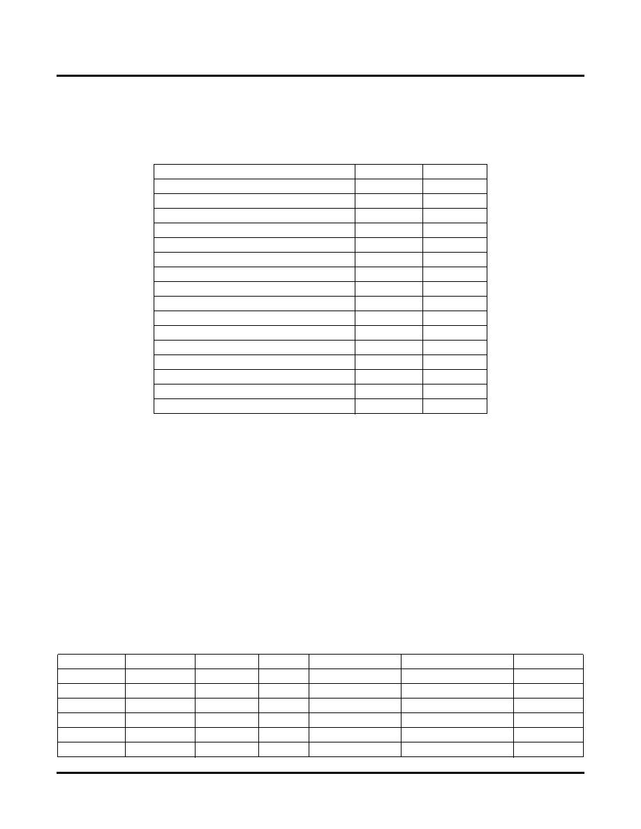
Table 50 provides the number of user-programmable I/Os available for each available package.
Table 50. I/O Summary
Table 51 provides the package pin and pin function for the ORSO42G5 and ORSO82G5 FPSC and packages. The
bond pad name is identied in the PIO nomenclature used in the ispLEVER System software design editor. The
Bank column provides information as to which output voltage level bank the given pin is in. The Group column pro-
vides information as to the group of pins the given pin is in. This is used to show which VREF pin is used to provide
the reference voltage for single-ended limited-swing I/Os. If none of these buffer types (such as SSTL, GTL, HSTL)
are used in a given group, then the VREF pin is available as an I/O pin.
When the number of FPGA bond pads exceeds the number of package pins, bond pads are unused. When the
number of package pins exceeds the number of bond pads, package pins are left unconnected (no connects).
When a package pin is to be left as a no connect for a specic die, it is indicated as a note in the device column for
the FPGA. The tables provide no information on unused pads.
The differential pairs within each bank are physically arranged so that the ball locations for the pair are adjacent in
either the horizontal, vertical or diagonal directions.
VREF pins, shown in the Pin Description columns in Table 51 are associated to the bank and group (e.g.,
VREF_TL_01 is the VREF for group one of the Top Left (TL) bank.
Device
ORSO42G5
ORSO82G5
User programmable I/O
204
372
Available programmable differential pair pins
166
330
FPGA conguration pins
7
FPGA dedicated function pins
2
Core function pins
32
71
VDD15
49
63
VDD33
8
10
VDDIO
34
32
VSS
112
91
VDDGB
2
VDDIB
4
8
VDDOB
8
12
VDD_ANA
22
8
Core LV_REF pins
1
No connect
0
2
Total package pins
484
680
Table 51. ORSO42G5 484-pin PBGAM Pinout
484-PBGAM
VDDIO Bank
VREF Group
I/O
Pin Description
Additional Function
484-PBGAM
E4
-
O
PRD_DATA
RD_DATA/TDO
-
C20
-
VDD15
-
D3
-
I
PRESET_N
RESET_N
-
F5
-
I
PRD_CFG_N
RD_CFG_N
-
F4
-
I
PPRGRM_N
PRGRM_N
-
C2
0 (TL)
7
IO
PL2D
PLL_CK0C/HPPLL
L1C
相关PDF资料 |
PDF描述 |
|---|---|
| EEM22DTAT-S189 | CONN EDGECARD 44POS R/A .156 SLD |
| ECC20DRES | CONN EDGECARD 40POS .100 EYELET |
| AT-S-26-4/4/W-25-R | MOD CORD STANDARD 4-4 WHITE 25' |
| EEC40DREI | CONN EDGECARD 80POS .100 EYELET |
| 0210490869 | CABLE JUMPER 1.25MM .203M 17POS |
相关代理商/技术参数 |
参数描述 |
|---|---|
| ORSO82G5 | 制造商:LATTICE 制造商全称:Lattice Semiconductor 功能描述:0.6 to 2.7 Gbps SONET Backplane Interface FPSCs |
| ORSO82G5-1BM680C | 功能描述:FPGA - 现场可编程门阵列 10368 LUT 372 I/O RoHS:否 制造商:Altera Corporation 系列:Cyclone V E 栅极数量: 逻辑块数量:943 内嵌式块RAM - EBR:1956 kbit 输入/输出端数量:128 最大工作频率:800 MHz 工作电源电压:1.1 V 最大工作温度:+ 70 C 安装风格:SMD/SMT 封装 / 箱体:FBGA-256 |
| ORSO82G5-1BM680I | 功能描述:FPGA - 现场可编程门阵列 10368 LUT 372 I/O RoHS:否 制造商:Altera Corporation 系列:Cyclone V E 栅极数量: 逻辑块数量:943 内嵌式块RAM - EBR:1956 kbit 输入/输出端数量:128 最大工作频率:800 MHz 工作电源电压:1.1 V 最大工作温度:+ 70 C 安装风格:SMD/SMT 封装 / 箱体:FBGA-256 |
| ORSO82G5-1F680C | 功能描述:FPGA - 现场可编程门阵列 ORCA FPSC 2.7GBITS/s BP XCVR 643K RoHS:否 制造商:Altera Corporation 系列:Cyclone V E 栅极数量: 逻辑块数量:943 内嵌式块RAM - EBR:1956 kbit 输入/输出端数量:128 最大工作频率:800 MHz 工作电源电压:1.1 V 最大工作温度:+ 70 C 安装风格:SMD/SMT 封装 / 箱体:FBGA-256 |
| ORSO82G5-1F680I | 功能描述:FPGA - 现场可编程门阵列 ORCA FPSC 2.7Gbits/s BP XCVR 643K RoHS:否 制造商:Altera Corporation 系列:Cyclone V E 栅极数量: 逻辑块数量:943 内嵌式块RAM - EBR:1956 kbit 输入/输出端数量:128 最大工作频率:800 MHz 工作电源电压:1.1 V 最大工作温度:+ 70 C 安装风格:SMD/SMT 封装 / 箱体:FBGA-256 |
发布紧急采购,3分钟左右您将得到回复。