- 您现在的位置:买卖IC网 > PDF目录17102 > ORSO42G5-EV (Lattice Semiconductor Corporation)BOARD EVAL DEV PLATFORM ORSO42G5 PDF资料下载
参数资料
| 型号: | ORSO42G5-EV |
| 厂商: | Lattice Semiconductor Corporation |
| 文件页数: | 146/153页 |
| 文件大小: | 0K |
| 描述: | BOARD EVAL DEV PLATFORM ORSO42G5 |
| 标准包装: | 1 |
| 系列: | ORCA® 4 系列 |
| 类型: | FPGA |
| 适用于相关产品: | ORSO42G5 |
| 所含物品: | 板,线缆,电源 |
| 其它名称: | ORSO42G5EV |
第1页第2页第3页第4页第5页第6页第7页第8页第9页第10页第11页第12页第13页第14页第15页第16页第17页第18页第19页第20页第21页第22页第23页第24页第25页第26页第27页第28页第29页第30页第31页第32页第33页第34页第35页第36页第37页第38页第39页第40页第41页第42页第43页第44页第45页第46页第47页第48页第49页第50页第51页第52页第53页第54页第55页第56页第57页第58页第59页第60页第61页第62页第63页第64页第65页第66页第67页第68页第69页第70页第71页第72页第73页第74页第75页第76页第77页第78页第79页第80页第81页第82页第83页第84页第85页第86页第87页第88页第89页第90页第91页第92页第93页第94页第95页第96页第97页第98页第99页第100页第101页第102页第103页第104页第105页第106页第107页第108页第109页第110页第111页第112页第113页第114页第115页第116页第117页第118页第119页第120页第121页第122页第123页第124页第125页第126页第127页第128页第129页第130页第131页第132页第133页第134页第135页第136页第137页第138页第139页第140页第141页第142页第143页第144页第145页当前第146页第147页第148页第149页第150页第151页第152页第153页
Lattice Semiconductor
ORCA ORSO42G5 and ORSO82G5 Data Sheet
92
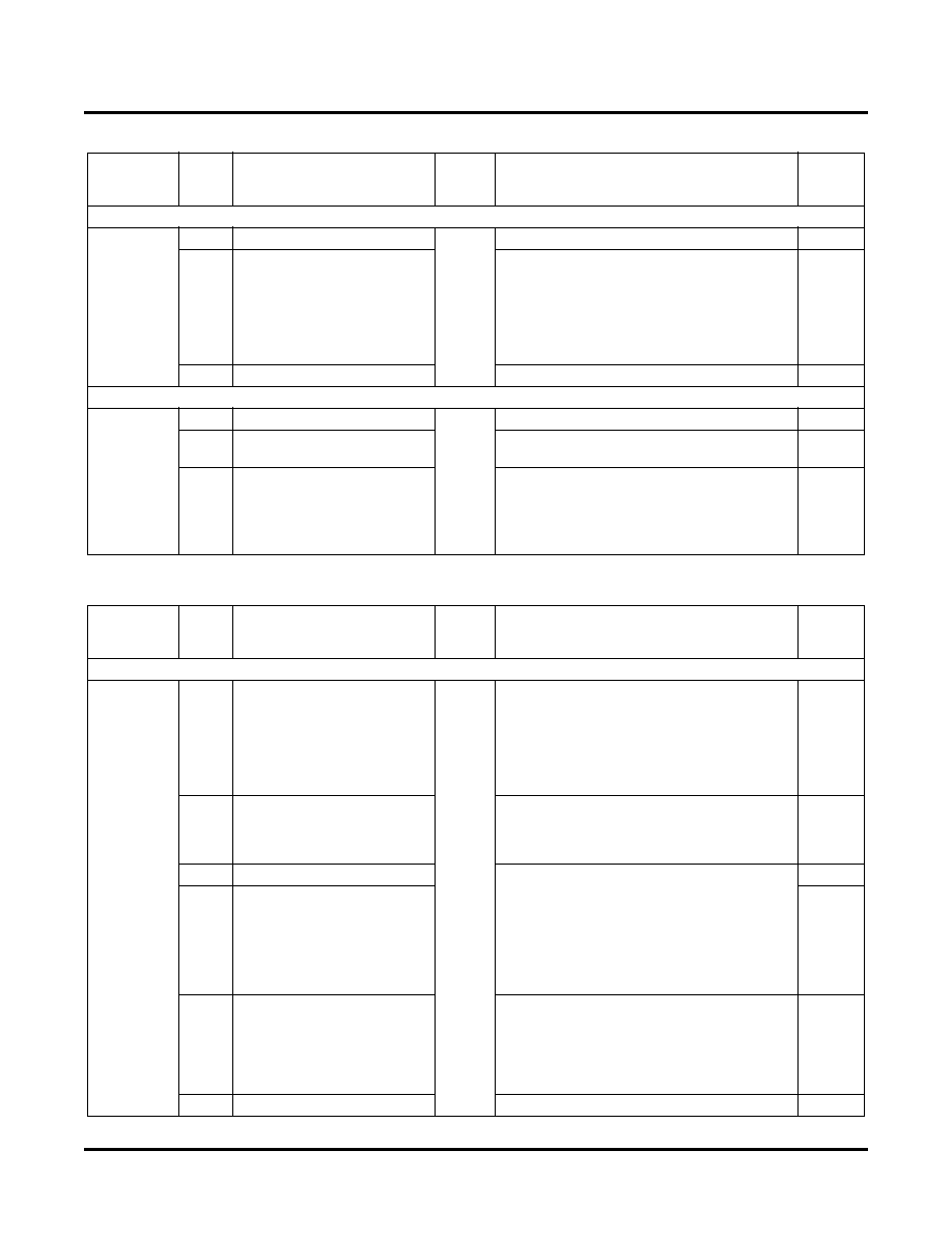
Table 29. SERDES Alarm and Alarm Mask Register Descriptions – ORSO82G5
Table 30. SERDES Per-Channel Transmit Conguration Register Descriptions – ORSO82G5
(0x)
Absolute
Address
Bit
Name
Reset
Value
(0x)
Description
Mode
SERDES Alarm Registers (Read Only) xx = [AA,...,BD]
30000 - AA
30010 - AB
30020 - AC
30030 - AD
30100 - BA
30110 - BB
30120 - BC
30130 - BD
[0]
RSVD
00
Reserved - May be non-zero
—
[1]
LKI_xx
Receive PLL Lock Indication, Channel xx.
LKI_xx = 1 indicates the receive PLL is locked.
Note that the PLL can either lock to the incom-
ing data or to RECLK_[A:B]. If the PLL is locked
to data and the data stream is terminated,
LKI_xx will go low until the PLL locks to
REFCLK_[A:B].
Both
[2:7]
RSVD
Reserved - May be non-zero
—
SERDES Alarm Mask Registers (Read/Write) xx = [AA,...,BD]
30001 - AA
30011 - AB
30021 - AC
30031 - AD
30101 - BA
30111 - BB
30121 - BC
30131 - BD
[0]
RSVD
FF
Reserved
—
[1]
MLKI_xx
Mask Receive PLL Lock Indication, Channel
MLKI_xx = 1 indicates LKI_xx is enabled
Both
[2:7]
RSVD
Reserved
—
(0x)
Absolute
Address
Bit
Name
Reset
Value
(0x)
Description
Mode
SERDES Transmit Per-Channel Conguration Registers (Read/Write) xx = [AA,...,BD]
30002 - AA
30012 - AB
30022 - AC
30032 - AD
30102 - BA
30112 - BB
30122 - BC
30132 - BD
[0]
TXHR_xx
00
Transmit Half Rate Selection Bit, Channel xx.
When TXHR_xx = 1, HDOUT_xx's baud rate =
(REFCLK[A:B]*8) and TCK78[A:B] =(REF-
CLK[A:B]/4); when TXHR_xx=0, HDOUT_xx's
baud rate = (REFCLK[A:B]*16) and
TCK78[A:B]=(REFCLK[A:B]/2).
TXHR_xx = 0 on device reset.
Both
[1]
PWRDNT_xx
Transmit Powerdown Control Bit, Channel xx.
When PWRDNT_xx = 1, sections of the trans-
mit hardware are powered down.
PWRDNT_xx = 0 on device reset.
Both
[2]
PE0_xx
Transmit Preemphasis Selection Bit 0, Channel
xx. PE0_xx and PE1_xx select one of three pre-
emphasis settings for the transmit section.
PEO_xx=PE1_xx = 0, Preemphasis is 0%
PEO_xx=1, PE1_xx = 0 or PEO_xx=0,
PE1_xx = 1, Preemphasis is 12.5%
PEO_xx=PE1_xx = 1, Preemphasis is 25%.
PEO_xx=PE1_xx = 0 on device reset.
Both
[3]
PE1_xx
Both
[4]
HAMP_xx
Transmit Half Amplitude Selection Bit, Channel
xx. When HAMP_xx = 1, the transmit output
buffer voltage swing is limited to half its normal
amplitude. Otherwise, the transmit output buffer
maintains its full voltage swing.
HAMP_xx = 0 on device reset.
Both
[5:7]
RSVD
Reserved, Always set to “000”
—
相关PDF资料 |
PDF描述 |
|---|---|
| EEM22DTAT-S189 | CONN EDGECARD 44POS R/A .156 SLD |
| ECC20DRES | CONN EDGECARD 40POS .100 EYELET |
| AT-S-26-4/4/W-25-R | MOD CORD STANDARD 4-4 WHITE 25' |
| EEC40DREI | CONN EDGECARD 80POS .100 EYELET |
| 0210490869 | CABLE JUMPER 1.25MM .203M 17POS |
相关代理商/技术参数 |
参数描述 |
|---|---|
| ORSO82G5 | 制造商:LATTICE 制造商全称:Lattice Semiconductor 功能描述:0.6 to 2.7 Gbps SONET Backplane Interface FPSCs |
| ORSO82G5-1BM680C | 功能描述:FPGA - 现场可编程门阵列 10368 LUT 372 I/O RoHS:否 制造商:Altera Corporation 系列:Cyclone V E 栅极数量: 逻辑块数量:943 内嵌式块RAM - EBR:1956 kbit 输入/输出端数量:128 最大工作频率:800 MHz 工作电源电压:1.1 V 最大工作温度:+ 70 C 安装风格:SMD/SMT 封装 / 箱体:FBGA-256 |
| ORSO82G5-1BM680I | 功能描述:FPGA - 现场可编程门阵列 10368 LUT 372 I/O RoHS:否 制造商:Altera Corporation 系列:Cyclone V E 栅极数量: 逻辑块数量:943 内嵌式块RAM - EBR:1956 kbit 输入/输出端数量:128 最大工作频率:800 MHz 工作电源电压:1.1 V 最大工作温度:+ 70 C 安装风格:SMD/SMT 封装 / 箱体:FBGA-256 |
| ORSO82G5-1F680C | 功能描述:FPGA - 现场可编程门阵列 ORCA FPSC 2.7GBITS/s BP XCVR 643K RoHS:否 制造商:Altera Corporation 系列:Cyclone V E 栅极数量: 逻辑块数量:943 内嵌式块RAM - EBR:1956 kbit 输入/输出端数量:128 最大工作频率:800 MHz 工作电源电压:1.1 V 最大工作温度:+ 70 C 安装风格:SMD/SMT 封装 / 箱体:FBGA-256 |
| ORSO82G5-1F680I | 功能描述:FPGA - 现场可编程门阵列 ORCA FPSC 2.7Gbits/s BP XCVR 643K RoHS:否 制造商:Altera Corporation 系列:Cyclone V E 栅极数量: 逻辑块数量:943 内嵌式块RAM - EBR:1956 kbit 输入/输出端数量:128 最大工作频率:800 MHz 工作电源电压:1.1 V 最大工作温度:+ 70 C 安装风格:SMD/SMT 封装 / 箱体:FBGA-256 |
发布紧急采购,3分钟左右您将得到回复。