- 您现在的位置:买卖IC网 > PDF目录17102 > ORSO42G5-EV (Lattice Semiconductor Corporation)BOARD EVAL DEV PLATFORM ORSO42G5 PDF资料下载
参数资料
| 型号: | ORSO42G5-EV |
| 厂商: | Lattice Semiconductor Corporation |
| 文件页数: | 84/153页 |
| 文件大小: | 0K |
| 描述: | BOARD EVAL DEV PLATFORM ORSO42G5 |
| 标准包装: | 1 |
| 系列: | ORCA® 4 系列 |
| 类型: | FPGA |
| 适用于相关产品: | ORSO42G5 |
| 所含物品: | 板,线缆,电源 |
| 其它名称: | ORSO42G5EV |
第1页第2页第3页第4页第5页第6页第7页第8页第9页第10页第11页第12页第13页第14页第15页第16页第17页第18页第19页第20页第21页第22页第23页第24页第25页第26页第27页第28页第29页第30页第31页第32页第33页第34页第35页第36页第37页第38页第39页第40页第41页第42页第43页第44页第45页第46页第47页第48页第49页第50页第51页第52页第53页第54页第55页第56页第57页第58页第59页第60页第61页第62页第63页第64页第65页第66页第67页第68页第69页第70页第71页第72页第73页第74页第75页第76页第77页第78页第79页第80页第81页第82页第83页当前第84页第85页第86页第87页第88页第89页第90页第91页第92页第93页第94页第95页第96页第97页第98页第99页第100页第101页第102页第103页第104页第105页第106页第107页第108页第109页第110页第111页第112页第113页第114页第115页第116页第117页第118页第119页第120页第121页第122页第123页第124页第125页第126页第127页第128页第129页第130页第131页第132页第133页第134页第135页第136页第137页第138页第139页第140页第141页第142页第143页第144页第145页第146页第147页第148页第149页第150页第151页第152页第153页
Lattice Semiconductor
ORCA ORSO42G5 and ORSO82G5 Data Sheet
36
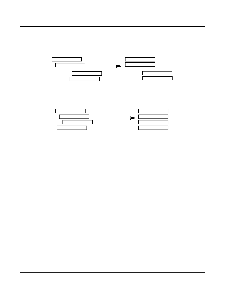
aligned together, channels C and D to form a pair as shown in Figure 20. Alternately, all four channels in the SER-
DES blocks can be aligned together to form a communication channel with a bandwidth of 10 Gbps as shown in
Figure 20. Twin Channel Alignment – ORSO42G5
Figure 21. Quad Channel Alignment of SERDES Blocks A and B – ORSO42G5
Individual channels within an alignment group can be disabled (i.e., powered-down) without disrupting other chan-
nels. Note that the SERDES channel that is powered down can not be the source of the RSYSCLKxx that is clock-
ing the read side of the alignment FIFO. When a disabled channel becomes active as part of an alignment group,
the group may need to be re-aligned. Then the whole group needs to be resynched. This would only need to occur
if the transmitting frame pulse for the new link is different from the rest of the group.
Each channel is provided with a 24 word x 33-bit FIFO. The FIFO can perform two tasks: (1) to change the clock
domain from receive clock to a clock from the FPGA side, and (2) to align the receive data over 2 or 4 channels.
This FIFO allows a timing budget of 307 ns that can be allocated to skew between the data lanes and for transfer to
the common clock. The input to the FIFO consists of 32-bit data and a frame pulse that indicates the start of a
frame (or A1A2 framing bytes). This frame pulse is used to synchronize multiple channels within an alignment
group.
If a channel is not in any alignment group, the FIFO control logic will set the FIFO-write-address to the beginning of
the FIFO, and will set the FIFO-read-address to the middle of the FIFO at the rst assertion of frame pulse after
reset or after the resync command.
The RX_FIFO_MIN register bits can be used to control the threshold for minimum unused buffer space in the align-
ment FIFOs between read and write pointers before OVFL status is agged. The synchronization algorithm con-
sists of a down counter which starts to count down by 1 from its initial value of 18 (decimal) when a frame pulse
from any channel within an alignment group has been received. The OOS alarm indicates the FIFO is out-of sync
and the channel skew exceeds that which can be handled by the FIFO. Once the frame pulse for all channels within
the alignment group have been received, the count is decremented by 2 until 0 is reached. Data are then read from
the FIFOs and output to the SPE generator before being sent to the FPGA.
For every alignment group, there is an OVFL and OOS status register bit. The OOS bit is agged when the down
counter in the synchronization algorithm has reached a value of 0 and frame pulse from all channels within an
alignment group have not been received. The OVFL bit is agged when the read address at the time of receiving a
Channel AC
Channel AD
Channel BC
Channel BD
Channel AC
Channel AD
t0
t1
OF CHANNELS AC AND AD
TWIN ALIGNMENT
OF CHANNELS BC AND BD
Channel BC
Channel BD
Channel AC
Channel AD
Channel BC
Channel BD
Channel AC
Channel AD
Channel BC
Channel BD
t0
QUAD ALIGNMENT OF CHANNELS AC
, AD, BC, AND BD
相关PDF资料 |
PDF描述 |
|---|---|
| EEM22DTAT-S189 | CONN EDGECARD 44POS R/A .156 SLD |
| ECC20DRES | CONN EDGECARD 40POS .100 EYELET |
| AT-S-26-4/4/W-25-R | MOD CORD STANDARD 4-4 WHITE 25' |
| EEC40DREI | CONN EDGECARD 80POS .100 EYELET |
| 0210490869 | CABLE JUMPER 1.25MM .203M 17POS |
相关代理商/技术参数 |
参数描述 |
|---|---|
| ORSO82G5 | 制造商:LATTICE 制造商全称:Lattice Semiconductor 功能描述:0.6 to 2.7 Gbps SONET Backplane Interface FPSCs |
| ORSO82G5-1BM680C | 功能描述:FPGA - 现场可编程门阵列 10368 LUT 372 I/O RoHS:否 制造商:Altera Corporation 系列:Cyclone V E 栅极数量: 逻辑块数量:943 内嵌式块RAM - EBR:1956 kbit 输入/输出端数量:128 最大工作频率:800 MHz 工作电源电压:1.1 V 最大工作温度:+ 70 C 安装风格:SMD/SMT 封装 / 箱体:FBGA-256 |
| ORSO82G5-1BM680I | 功能描述:FPGA - 现场可编程门阵列 10368 LUT 372 I/O RoHS:否 制造商:Altera Corporation 系列:Cyclone V E 栅极数量: 逻辑块数量:943 内嵌式块RAM - EBR:1956 kbit 输入/输出端数量:128 最大工作频率:800 MHz 工作电源电压:1.1 V 最大工作温度:+ 70 C 安装风格:SMD/SMT 封装 / 箱体:FBGA-256 |
| ORSO82G5-1F680C | 功能描述:FPGA - 现场可编程门阵列 ORCA FPSC 2.7GBITS/s BP XCVR 643K RoHS:否 制造商:Altera Corporation 系列:Cyclone V E 栅极数量: 逻辑块数量:943 内嵌式块RAM - EBR:1956 kbit 输入/输出端数量:128 最大工作频率:800 MHz 工作电源电压:1.1 V 最大工作温度:+ 70 C 安装风格:SMD/SMT 封装 / 箱体:FBGA-256 |
| ORSO82G5-1F680I | 功能描述:FPGA - 现场可编程门阵列 ORCA FPSC 2.7Gbits/s BP XCVR 643K RoHS:否 制造商:Altera Corporation 系列:Cyclone V E 栅极数量: 逻辑块数量:943 内嵌式块RAM - EBR:1956 kbit 输入/输出端数量:128 最大工作频率:800 MHz 工作电源电压:1.1 V 最大工作温度:+ 70 C 安装风格:SMD/SMT 封装 / 箱体:FBGA-256 |
发布紧急采购,3分钟左右您将得到回复。