- 您现在的位置:买卖IC网 > PDF目录17102 > ORSO42G5-EV (Lattice Semiconductor Corporation)BOARD EVAL DEV PLATFORM ORSO42G5 PDF资料下载
参数资料
| 型号: | ORSO42G5-EV |
| 厂商: | Lattice Semiconductor Corporation |
| 文件页数: | 19/153页 |
| 文件大小: | 0K |
| 描述: | BOARD EVAL DEV PLATFORM ORSO42G5 |
| 标准包装: | 1 |
| 系列: | ORCA® 4 系列 |
| 类型: | FPGA |
| 适用于相关产品: | ORSO42G5 |
| 所含物品: | 板,线缆,电源 |
| 其它名称: | ORSO42G5EV |
第1页第2页第3页第4页第5页第6页第7页第8页第9页第10页第11页第12页第13页第14页第15页第16页第17页第18页当前第19页第20页第21页第22页第23页第24页第25页第26页第27页第28页第29页第30页第31页第32页第33页第34页第35页第36页第37页第38页第39页第40页第41页第42页第43页第44页第45页第46页第47页第48页第49页第50页第51页第52页第53页第54页第55页第56页第57页第58页第59页第60页第61页第62页第63页第64页第65页第66页第67页第68页第69页第70页第71页第72页第73页第74页第75页第76页第77页第78页第79页第80页第81页第82页第83页第84页第85页第86页第87页第88页第89页第90页第91页第92页第93页第94页第95页第96页第97页第98页第99页第100页第101页第102页第103页第104页第105页第106页第107页第108页第109页第110页第111页第112页第113页第114页第115页第116页第117页第118页第119页第120页第121页第122页第123页第124页第125页第126页第127页第128页第129页第130页第131页第132页第133页第134页第135页第136页第137页第138页第139页第140页第141页第142页第143页第144页第145页第146页第147页第148页第149页第150页第151页第152页第153页
Lattice Semiconductor
ORCA ORSO42G5 and ORSO82G5 Data Sheet
115
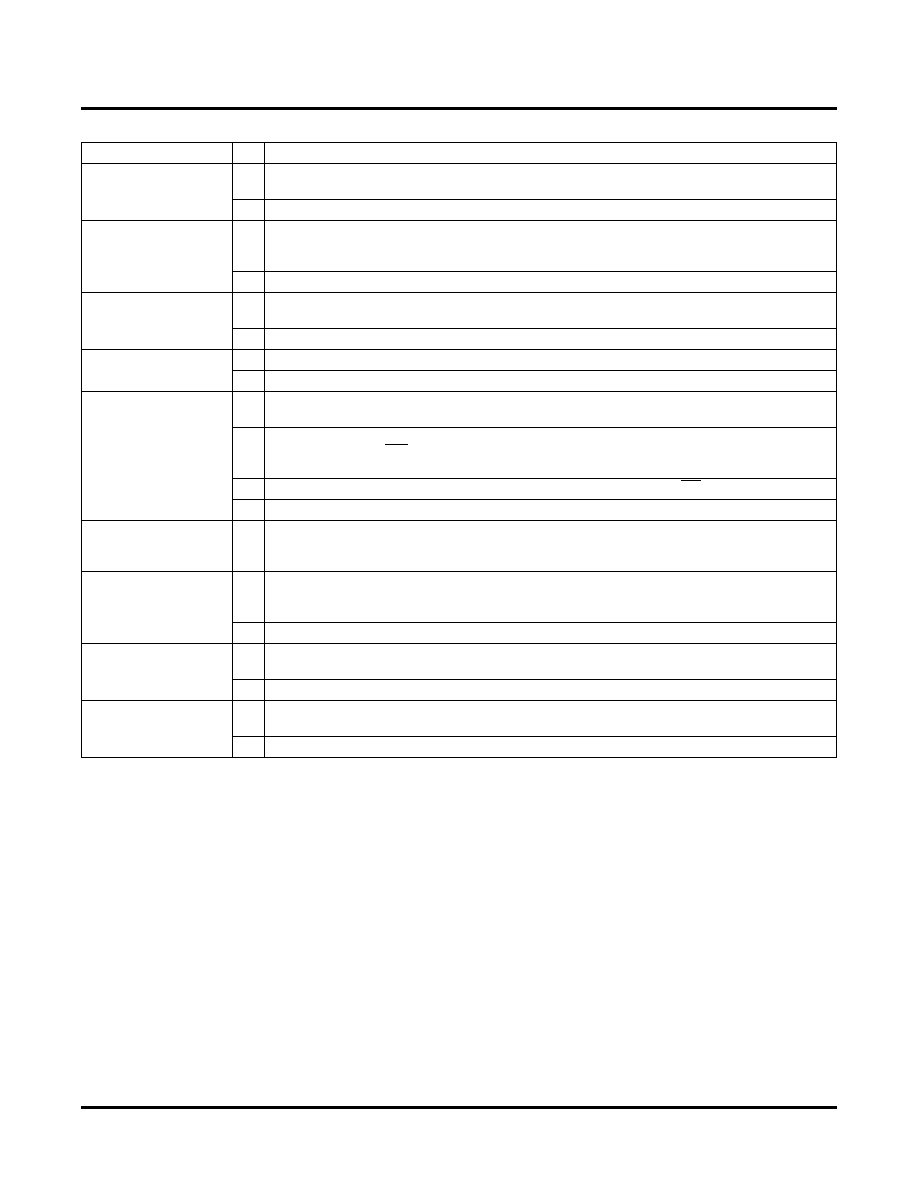
MPI_ACK
O
In
MPI mode this is driven low indicating the MPI received the data on the write cycle or
returned data on a read cycle.
I/O If not used for MPI these pins are user-programmable I/O pins after conguration.
1
MPI_CLK
I
This is the PowerPC synchronous, positive-edge bus clock used for the
MPI interface. It can be
a source of the clock for the Embedded System Bus. If MPI is used this will be the AMBA bus
clock.
I/O If not used for MPI these pins are user-programmable I/O pins after conguration.
1
MPI_TEA
O
A low on the MPI transfer error acknowledge indicates that the MPI detects a bus error on the
internal system bus for the current transaction.
I/O If not used for MPI these pins are user-programmable I/O pins after conguration.
1
MPI_RTRY
O
This pin requests the MPC860 to relinquish the bus and retry the cycle.
I/O If not used for MPI these pins are user-programmable I/O pins after conguration.
1
D[0:31]
I/O Selectable data bu
s width from 8, 16, 32-bit in MPI mode. Driven by the bus master in a write
transaction and driven by MPI in a read transaction.
I
D[7:0] receive conguration data during master parallel, peripheral, and slave parallel congu-
ration modes when WR is low and each pin has a pull-up enabled. During serial conguration
modes, D0 is the DIN input.
O
D[7:3] output internal status for asynchronous peripheral mode when RD is low.
I/O After conguration, if MPI is not used, the pins are user-programmable I/O pins.
1
DP[0:3]
I/O Selectable parity bus width in MPI mode from 1, 2, 4-bit, DP[0] for D[0:7], DP[1] for D[8:15],
DP[2] for D[16:23], and DP[3] for D[24:31].
After conguration, if MPI is not used, the pins are user-programmable I/O pin.
1
DIN
I
During slave serial or master serial conguration modes, DIN accepts serial conguration data
synchronous with CCLK. During parallel conguration modes, DIN is the D0 input. During con-
guration, a pull-up is enabled.
I/O After conguration, this pin is a user-programmable I/O pin.
1
DOUT
O
During conguration, DOUT is the serial data output that can drive the DIN of daisy-chained
slave devices. Data out on DOUT changes on the rising edge of CCLK.
I/O After conguration, DOUT is a user-programmable I/O pin.
1
TESTCFG
(ORSO82G5 only)
I
During conguration this pin should be held high, to allow conguration to occur. A pull up is
enabled during conguration.
I/O After conguration, TESTCFG is a user programmable I/O pin.
1
1. The FPGA States of Operation section in the ORCA Series 4 FPGAs data sheet contains more information on how to control these signals
during start-up. The timing of DONE release is controlled by one set of bit stream options, and the timing of the simultaneous release of all
other conguration pins (and the activation of all user I/Os) is controlled by a second set of options.
Table 47. Pin Descriptions (Continued)
Symbol
I/O
Description
相关PDF资料 |
PDF描述 |
|---|---|
| EEM22DTAT-S189 | CONN EDGECARD 44POS R/A .156 SLD |
| ECC20DRES | CONN EDGECARD 40POS .100 EYELET |
| AT-S-26-4/4/W-25-R | MOD CORD STANDARD 4-4 WHITE 25' |
| EEC40DREI | CONN EDGECARD 80POS .100 EYELET |
| 0210490869 | CABLE JUMPER 1.25MM .203M 17POS |
相关代理商/技术参数 |
参数描述 |
|---|---|
| ORSO82G5 | 制造商:LATTICE 制造商全称:Lattice Semiconductor 功能描述:0.6 to 2.7 Gbps SONET Backplane Interface FPSCs |
| ORSO82G5-1BM680C | 功能描述:FPGA - 现场可编程门阵列 10368 LUT 372 I/O RoHS:否 制造商:Altera Corporation 系列:Cyclone V E 栅极数量: 逻辑块数量:943 内嵌式块RAM - EBR:1956 kbit 输入/输出端数量:128 最大工作频率:800 MHz 工作电源电压:1.1 V 最大工作温度:+ 70 C 安装风格:SMD/SMT 封装 / 箱体:FBGA-256 |
| ORSO82G5-1BM680I | 功能描述:FPGA - 现场可编程门阵列 10368 LUT 372 I/O RoHS:否 制造商:Altera Corporation 系列:Cyclone V E 栅极数量: 逻辑块数量:943 内嵌式块RAM - EBR:1956 kbit 输入/输出端数量:128 最大工作频率:800 MHz 工作电源电压:1.1 V 最大工作温度:+ 70 C 安装风格:SMD/SMT 封装 / 箱体:FBGA-256 |
| ORSO82G5-1F680C | 功能描述:FPGA - 现场可编程门阵列 ORCA FPSC 2.7GBITS/s BP XCVR 643K RoHS:否 制造商:Altera Corporation 系列:Cyclone V E 栅极数量: 逻辑块数量:943 内嵌式块RAM - EBR:1956 kbit 输入/输出端数量:128 最大工作频率:800 MHz 工作电源电压:1.1 V 最大工作温度:+ 70 C 安装风格:SMD/SMT 封装 / 箱体:FBGA-256 |
| ORSO82G5-1F680I | 功能描述:FPGA - 现场可编程门阵列 ORCA FPSC 2.7Gbits/s BP XCVR 643K RoHS:否 制造商:Altera Corporation 系列:Cyclone V E 栅极数量: 逻辑块数量:943 内嵌式块RAM - EBR:1956 kbit 输入/输出端数量:128 最大工作频率:800 MHz 工作电源电压:1.1 V 最大工作温度:+ 70 C 安装风格:SMD/SMT 封装 / 箱体:FBGA-256 |
发布紧急采购,3分钟左右您将得到回复。