- 您现在的位置:买卖IC网 > PDF目录17102 > ORSO42G5-EV (Lattice Semiconductor Corporation)BOARD EVAL DEV PLATFORM ORSO42G5 PDF资料下载
参数资料
| 型号: | ORSO42G5-EV |
| 厂商: | Lattice Semiconductor Corporation |
| 文件页数: | 94/153页 |
| 文件大小: | 0K |
| 描述: | BOARD EVAL DEV PLATFORM ORSO42G5 |
| 标准包装: | 1 |
| 系列: | ORCA® 4 系列 |
| 类型: | FPGA |
| 适用于相关产品: | ORSO42G5 |
| 所含物品: | 板,线缆,电源 |
| 其它名称: | ORSO42G5EV |
第1页第2页第3页第4页第5页第6页第7页第8页第9页第10页第11页第12页第13页第14页第15页第16页第17页第18页第19页第20页第21页第22页第23页第24页第25页第26页第27页第28页第29页第30页第31页第32页第33页第34页第35页第36页第37页第38页第39页第40页第41页第42页第43页第44页第45页第46页第47页第48页第49页第50页第51页第52页第53页第54页第55页第56页第57页第58页第59页第60页第61页第62页第63页第64页第65页第66页第67页第68页第69页第70页第71页第72页第73页第74页第75页第76页第77页第78页第79页第80页第81页第82页第83页第84页第85页第86页第87页第88页第89页第90页第91页第92页第93页当前第94页第95页第96页第97页第98页第99页第100页第101页第102页第103页第104页第105页第106页第107页第108页第109页第110页第111页第112页第113页第114页第115页第116页第117页第118页第119页第120页第121页第122页第123页第124页第125页第126页第127页第128页第129页第130页第131页第132页第133页第134页第135页第136页第137页第138页第139页第140页第141页第142页第143页第144页第145页第146页第147页第148页第149页第150页第151页第152页第153页
Lattice Semiconductor
ORCA ORSO42G5 and ORSO82G5 Data Sheet
45
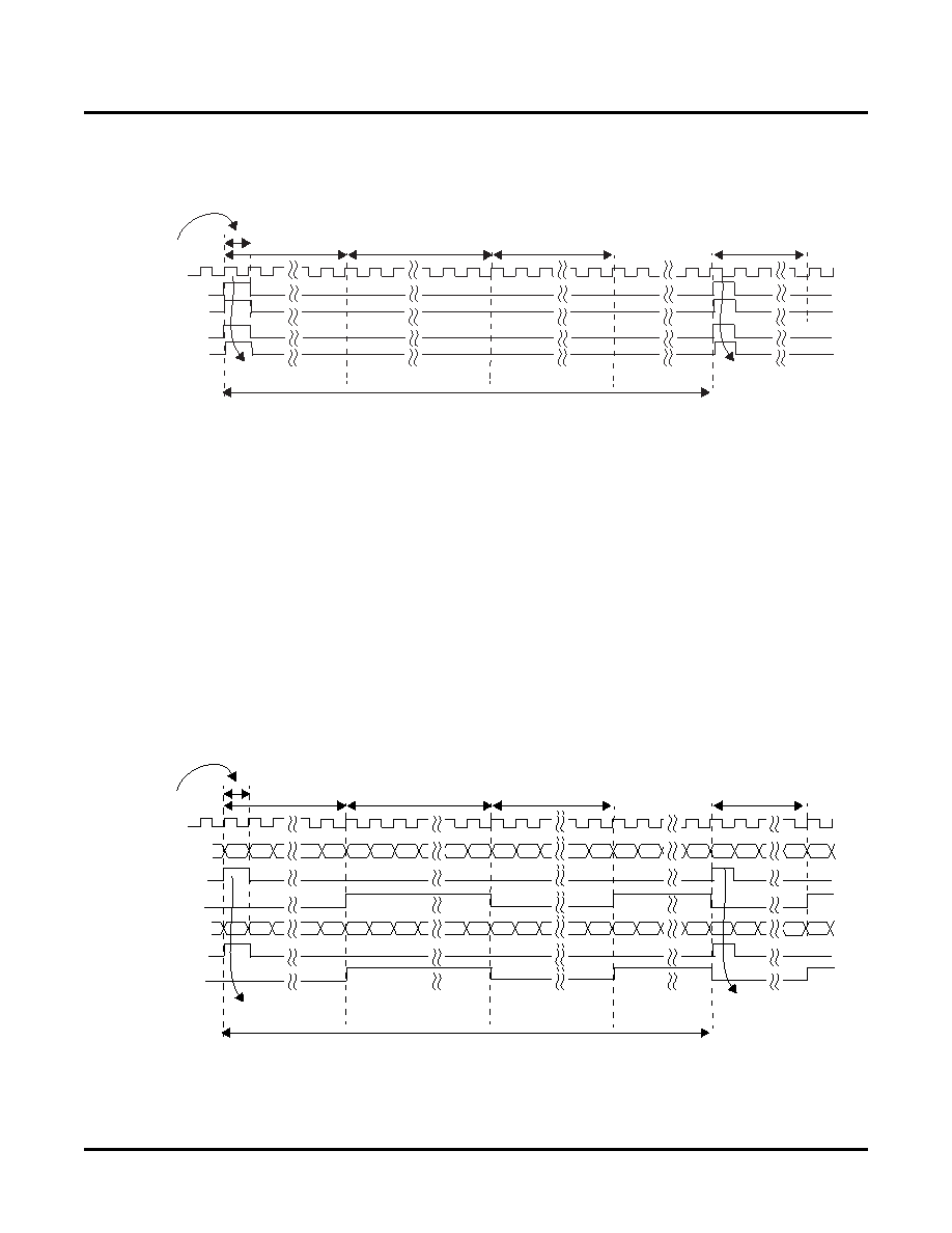
Figure 31 shows the quad alignment mode in the ORSO42G5.
Figure 31. Receive SONET Mode, Quad Alignment Mode – ORSO42G5
SONET Mode Receive Timing – ORSO82G5
This section contains timing diagrams for major interfaces of this block to the FPGA logic when SONET frames are
to be transferred.
When operating in SONET mode, the entire SONET frame is sent to the FPGA. In multi-channel alignment
mode(s), data from all channels within an alignment group are aligned to the A1A2 framing bytes.
Each SONET frame is 125μs. The frame starts with 36 clock cycles (77.76 MHz) of TOH followed by 1044 clock
cycles of SPE, followed by 36 clock cycles of TOH, 1044 cycles of SPE.
The DOUTxx_SPE signal indicates TOH or SPE in the data (low for TOH, high for SPE)
Twin pairs are AA, AB (group A1), AC, AD (group A2), BA, BB (group B1) and BC, BD (group B2)
Figure 32 shows the SONET twin alignment mode timing for the ORSO82G5. The frame pulse and SPE indicators
are show for each of the two channels (AA, AB) in twin alignment.
Figure 32. Receive Clocking Diagram for SONET Mode Twin Alignment in Block A – ORSO82G5
...
1 cycle
36 cycles TOH
1044 cycles SPE
36 cycles TOH
Start of Frame
125 μs
Clocks
RSYSCLKA2 and RSYSYSCLKB2 are sourced by RCK78A
36 cycles TOH
Start of Frame
DOUTAC_FP
DOUTAD_FP
RSYSCLK[A2,B2]
DOUTBC_FP
DOUTBD_FP
RSYSCLKA1
DOUTAA[31:0]
DOUTAA_FP
TT
T
S
SS
T
SSSS
S
...
1 cycle
36 cycles TOH
1
044 cycles SPE
36 cycles TOH
Start of Frame
125 μs
Data
T Represents TOH
S Represents SPE
DOUTxx-SPE is high for SPE, low for TOH
Clocks
RSYSCLKA1 is the read clock used for group A1
RSYSCLKA2 is the read clock used for group A2
RSYSCLKB1 is the read clock used for group B1
RSYSBLKB2 is the read clock used for group B2
36 cycles TOH
TT
T
S
SS
T
SSSS
S
Start of Frame
DOUTAA_SPE
DOUTAB[31:0]
DOUTAB_SPE
DOUTAB_FP
相关PDF资料 |
PDF描述 |
|---|---|
| EEM22DTAT-S189 | CONN EDGECARD 44POS R/A .156 SLD |
| ECC20DRES | CONN EDGECARD 40POS .100 EYELET |
| AT-S-26-4/4/W-25-R | MOD CORD STANDARD 4-4 WHITE 25' |
| EEC40DREI | CONN EDGECARD 80POS .100 EYELET |
| 0210490869 | CABLE JUMPER 1.25MM .203M 17POS |
相关代理商/技术参数 |
参数描述 |
|---|---|
| ORSO82G5 | 制造商:LATTICE 制造商全称:Lattice Semiconductor 功能描述:0.6 to 2.7 Gbps SONET Backplane Interface FPSCs |
| ORSO82G5-1BM680C | 功能描述:FPGA - 现场可编程门阵列 10368 LUT 372 I/O RoHS:否 制造商:Altera Corporation 系列:Cyclone V E 栅极数量: 逻辑块数量:943 内嵌式块RAM - EBR:1956 kbit 输入/输出端数量:128 最大工作频率:800 MHz 工作电源电压:1.1 V 最大工作温度:+ 70 C 安装风格:SMD/SMT 封装 / 箱体:FBGA-256 |
| ORSO82G5-1BM680I | 功能描述:FPGA - 现场可编程门阵列 10368 LUT 372 I/O RoHS:否 制造商:Altera Corporation 系列:Cyclone V E 栅极数量: 逻辑块数量:943 内嵌式块RAM - EBR:1956 kbit 输入/输出端数量:128 最大工作频率:800 MHz 工作电源电压:1.1 V 最大工作温度:+ 70 C 安装风格:SMD/SMT 封装 / 箱体:FBGA-256 |
| ORSO82G5-1F680C | 功能描述:FPGA - 现场可编程门阵列 ORCA FPSC 2.7GBITS/s BP XCVR 643K RoHS:否 制造商:Altera Corporation 系列:Cyclone V E 栅极数量: 逻辑块数量:943 内嵌式块RAM - EBR:1956 kbit 输入/输出端数量:128 最大工作频率:800 MHz 工作电源电压:1.1 V 最大工作温度:+ 70 C 安装风格:SMD/SMT 封装 / 箱体:FBGA-256 |
| ORSO82G5-1F680I | 功能描述:FPGA - 现场可编程门阵列 ORCA FPSC 2.7Gbits/s BP XCVR 643K RoHS:否 制造商:Altera Corporation 系列:Cyclone V E 栅极数量: 逻辑块数量:943 内嵌式块RAM - EBR:1956 kbit 输入/输出端数量:128 最大工作频率:800 MHz 工作电源电压:1.1 V 最大工作温度:+ 70 C 安装风格:SMD/SMT 封装 / 箱体:FBGA-256 |
发布紧急采购,3分钟左右您将得到回复。