- 您现在的位置:买卖IC网 > PDF目录1987 > AD9547BCPZ-REEL7 (Analog Devices Inc)IC CLOCK GEN/SYNCHRONIZR 64LFCSP PDF资料下载
参数资料
| 型号: | AD9547BCPZ-REEL7 |
| 厂商: | Analog Devices Inc |
| 文件页数: | 30/104页 |
| 文件大小: | 0K |
| 描述: | IC CLOCK GEN/SYNCHRONIZR 64LFCSP |
| 产品变化通告: | AD9547 Mask Change 20/Oct/2010 |
| 标准包装: | 750 |
| 类型: | 时钟/频率发生器,同步器 |
| PLL: | 是 |
| 主要目的: | 以太网,SONET/SDH,Stratum |
| 输入: | CMOS,LVDS,LVPECL |
| 输出: | CMOS,LVDS,LVPECL |
| 电路数: | 1 |
| 比率 - 输入:输出: | 2:2 |
| 差分 - 输入:输出: | 是/是 |
| 频率 - 最大: | 750kHz |
| 电源电压: | 1.71 V ~ 3.465 V |
| 工作温度: | -40°C ~ 85°C |
| 安装类型: | 表面贴装 |
| 封装/外壳: | 64-VFQFN 裸露焊盘,CSP |
| 供应商设备封装: | 64-LFCSP-VQ(9x9) |
| 包装: | 带卷 (TR) |
第1页第2页第3页第4页第5页第6页第7页第8页第9页第10页第11页第12页第13页第14页第15页第16页第17页第18页第19页第20页第21页第22页第23页第24页第25页第26页第27页第28页第29页当前第30页第31页第32页第33页第34页第35页第36页第37页第38页第39页第40页第41页第42页第43页第44页第45页第46页第47页第48页第49页第50页第51页第52页第53页第54页第55页第56页第57页第58页第59页第60页第61页第62页第63页第64页第65页第66页第67页第68页第69页第70页第71页第72页第73页第74页第75页第76页第77页第78页第79页第80页第81页第82页第83页第84页第85页第86页第87页第88页第89页第90页第91页第92页第93页第94页第95页第96页第97页第98页第99页第100页第101页第102页第103页第104页
Data Sheet
AD9547
Rev. E | Page 31 of 104
A
ACTIVE
AA
ACTIVE
B
ACTIVE
A FAULTED
AA FAULTED
ALL VALID
INITIAL
STATE
A VALID
AA VALID
A VALID
AA VALID
INPUT
PRIORITY
PROMOTED
A0
0
AA
1
0
B2
1
BB
3
2
PRIORITY TABLE
COMMON
WITHOUT PROMOTION
WITH PROMOTION
08300-
011
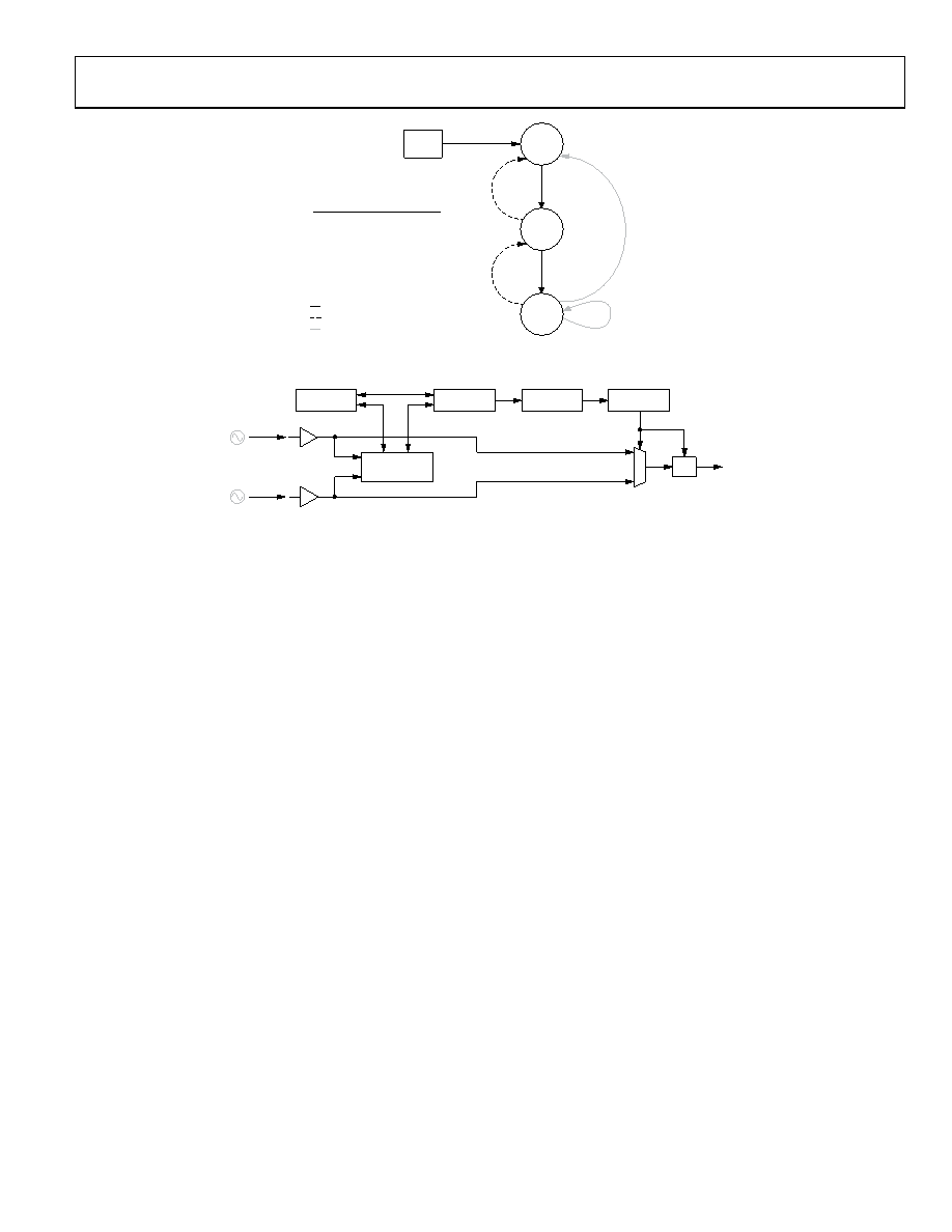
Figure 34. Example of Priority Promotion
PROFILE
SELECTION
VALIDATION
LOGIC
PRIORITY
SELECTION
÷R
MONITORS
REF A/REF AA
REF B/REF BB
TDC
LOOP
CONTROLLER
……
…
0830
0-
01
2
Figure 35. Reference Clock Block Diagram
The promoted priority parameter allows the user to assign a higher
priority to a reference after it becomes the active reference. For
example, suppose that two references have a selection priority of 3
and a promoted priority of 1, and the remaining references have
a selection priority of 2 and a promoted priority of 2. Now, assume
that one of the Priority 3 references becomes active because all
of the Priority 2 references have failed. Sometime later, however,
a Priority 2 reference becomes valid. The switchover logic normally
attempts to automatically switch over to the Priority 2 reference
because it has higher priority than the presently active Priority 3
reference. However, because the Priority 3 reference is active, its
promoted priority of 1 is in effect. This is a higher priority than
the newly validated reference’s priority of 2, so the switchover does
not occur. This mechanism enables the user to give references
preferential treatment while they are selected as the active refer-
ence. An example of promoted vs. nonpromoted priority switching
appears in state diagram form in. Figure 35 shows a block diagram
of the interrelationship between the reference inputs, monitors,
validation logic, profile selection, and priority selection
functionality.
Phase Build-Out Reference Switching
Phase build-out reference switching is the term given to a ref-
erence switchover that completely masks any phase difference
between the previous reference and the new reference. That is,
there is virtually no phase change that can be detected at the
output when a phase build-out switchover occurs.
The AD9547 handles phase build-out switching based on whether
the new reference is a phase master. A phase master is any reference
with a selection priority value that is less than the phase master
threshold priority value (that is, higher priority). The phase master
threshold priority value resides in the phase build-out switching
register (Address 0x0507), and the selection priority resides in the
profile registers (Address 0x0600 to Address 0x07FF). By default,
the phase master threshold priority is 0; therefore, no references
can be phase masters until the user changes the phase master
threshold priority.
When the AD9547 switches from one reference to another, it
compares the selection priority value that is stored in the profile
that is assigned to the new reference with the phase master
threshold priority. The AD9547 performs a phase build-out
switchover only if the new reference is not a phase master.
Hitless Reference Switching (Phase Slew Control)
Hitless reference switching is the term given to a reference switch-
over that limits the rate of change of the phase of the output clock
while the PLL is in the process of acquiring phase lock. This
prevents the output frequency offset from becoming excessive.
The all-digital nature of the DPLL core (see the Digital Phase-
Locked Loop (DPLL) Core section) gives the user numerical
control of the rate at which phase changes occur at the DPLL
output. When enabled, a phase slew controller monitors the
phase difference between the feedback and reference inputs to the
DPLL. The phase slew controller can place a user specified limit on
the rate of change of phase, thus providing a mechanism for
hitless reference switching.
The user sets a limit on the rate of change of phase by storing
the appropriate value in the 16-bit phase slew rate limit register
(Address 0x0316 and Address 0x0317). The 16-bit word, which
represents units of ns/sec, puts an upper bound on the rate of
change of the phase at the output of the DPLL during a reference
switchover. A phase slew rate value of 0 (default) disables the
phase slew controller.
The accuracy of the phase slew controller depends on both the
phase slew limit value and the system clock frequency. Generally,
相关PDF资料 |
PDF描述 |
|---|---|
| AD9548BCPZ-REEL7 | IC CLOCK GEN/SYNCHRONIZR 88LFCSP |
| AD9549ABCPZ-REEL7 | IC CLOCK GEN/SYNCHRONIZR 64LFCSP |
| AD9550BCPZ-REEL7 | IC INTEGER-N TRANSLATOR 32-LFCSP |
| AD9551BCPZ | IC CLOCK GEN MULTISERV 40-LFCSP |
| AD9552BCPZ-REEL7 | IC PLL CLOCK GEN LP 32LFCSP |
相关代理商/技术参数 |
参数描述 |
|---|---|
| AD9548 | 制造商:AD 制造商全称:Analog Devices 功能描述:Quad/Octal Input Network Clock Generator/Synchronizer |
| AD9548/PCBZ | 功能描述:BOARD EVAL FOR AD9548 RoHS:是 类别:编程器,开发系统 >> 评估演示板和套件 系列:- 标准包装:1 系列:PSoC® 主要目的:电源管理,热管理 嵌入式:- 已用 IC / 零件:- 主要属性:- 次要属性:- 已供物品:板,CD,电源 |
| AD9548/PCBZ | 制造商:Analog Devices 功能描述:Clock Generator Evaluation Board |
| AD9548BCPZ | 功能描述:IC CLOCK GEN/SYNCHRONIZR 88LFCSP RoHS:是 类别:集成电路 (IC) >> 时钟/计时 - 专用 系列:- 标准包装:1 系列:- 类型:时钟/频率发生器,多路复用器 PLL:是 主要目的:存储器,RDRAM 输入:晶体 输出:LVCMOS 电路数:1 比率 - 输入:输出:1:2 差分 - 输入:输出:无/是 频率 - 最大:400MHz 电源电压:3 V ~ 3.6 V 工作温度:0°C ~ 85°C 安装类型:表面贴装 封装/外壳:16-TSSOP(0.173",4.40mm 宽) 供应商设备封装:16-TSSOP 包装:Digi-Reel® 其它名称:296-6719-6 |
| AD9548BCPZ-REEL7 | 功能描述:IC CLOCK GEN/SYNCHRONIZR 88LFCSP RoHS:是 类别:集成电路 (IC) >> 时钟/计时 - 专用 系列:- 标准包装:28 系列:- 类型:时钟/频率发生器 PLL:是 主要目的:Intel CPU 服务器 输入:时钟 输出:LVCMOS 电路数:1 比率 - 输入:输出:3:22 差分 - 输入:输出:无/是 频率 - 最大:400MHz 电源电压:3.135 V ~ 3.465 V 工作温度:0°C ~ 85°C 安装类型:表面贴装 封装/外壳:64-TFSOP (0.240",6.10mm 宽) 供应商设备封装:64-TSSOP 包装:管件 |
发布紧急采购,3分钟左右您将得到回复。