- 您现在的位置:买卖IC网 > PDF目录1987 > AD9547BCPZ-REEL7 (Analog Devices Inc)IC CLOCK GEN/SYNCHRONIZR 64LFCSP PDF资料下载
参数资料
| 型号: | AD9547BCPZ-REEL7 |
| 厂商: | Analog Devices Inc |
| 文件页数: | 33/104页 |
| 文件大小: | 0K |
| 描述: | IC CLOCK GEN/SYNCHRONIZR 64LFCSP |
| 产品变化通告: | AD9547 Mask Change 20/Oct/2010 |
| 标准包装: | 750 |
| 类型: | 时钟/频率发生器,同步器 |
| PLL: | 是 |
| 主要目的: | 以太网,SONET/SDH,Stratum |
| 输入: | CMOS,LVDS,LVPECL |
| 输出: | CMOS,LVDS,LVPECL |
| 电路数: | 1 |
| 比率 - 输入:输出: | 2:2 |
| 差分 - 输入:输出: | 是/是 |
| 频率 - 最大: | 750kHz |
| 电源电压: | 1.71 V ~ 3.465 V |
| 工作温度: | -40°C ~ 85°C |
| 安装类型: | 表面贴装 |
| 封装/外壳: | 64-VFQFN 裸露焊盘,CSP |
| 供应商设备封装: | 64-LFCSP-VQ(9x9) |
| 包装: | 带卷 (TR) |
第1页第2页第3页第4页第5页第6页第7页第8页第9页第10页第11页第12页第13页第14页第15页第16页第17页第18页第19页第20页第21页第22页第23页第24页第25页第26页第27页第28页第29页第30页第31页第32页当前第33页第34页第35页第36页第37页第38页第39页第40页第41页第42页第43页第44页第45页第46页第47页第48页第49页第50页第51页第52页第53页第54页第55页第56页第57页第58页第59页第60页第61页第62页第63页第64页第65页第66页第67页第68页第69页第70页第71页第72页第73页第74页第75页第76页第77页第78页第79页第80页第81页第82页第83页第84页第85页第86页第87页第88页第89页第90页第91页第92页第93页第94页第95页第96页第97页第98页第99页第100页第101页第102页第103页第104页
AD9547
Data Sheet
Rev. E | Page 34 of 104
phase error sample but, rather, its magnitude relative tothe phase
threshold value that determines whether to fill or drain. If more
filling is taking place than draining, the water level in the tub
eventually rises above the high water mark (+1024), which causes
the phase lock detector toindicate lock. If more draining is taking
place than filling, the water levelin the tubeventually falls below
the low water mark (1024), which causes the phase lock detector
to indicate unlock. The ability to specify the threshold level, fill
rate, and drain rate enables the user to tailor the operation of
the phase lock detector to the statistics of the timing jitter
associated with the input reference signal.
Note that when the AD9547 enters the free-run or holdover
mode, the DPLL phase lock detector indicates unlocked. Also,
when the AD9547 performs a reference switchover, the state of
the lock detector prior to the switch is preserved during the
transition period.
DPLLFrequencyLock Detector
The operation of the frequency lock detector is identical to that
of the phase lock detector. The only difference is that the fill or
drain decision is based on the period deviation between the
reference and feedback signals of the DPLL instead of the phase
error at the output of the PFD.
The frequency lock detector uses a 24-bit frequency threshold
register specified in units of picoseconds (ps). Thus, the fre-
quency threshold value extends from 0 μs to ±16.777215 μs.
It represents the magnitude of the difference in period between
the reference and feedback signals at the input to the DPLL. For
example, if the reference signal is 1.25 MHz and the feedback
signal is 1.38 MHz, the period difference is approximately 75.36 ns
(|1/1,250,000 1/1,380,000| ≈ 75.36 ns).
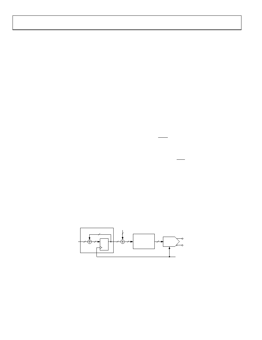
DIRECT DIGITAL SYNTHESIZER (DDS)
DDS Overview
One of the primary building blocks of the digital PLL is a direct
digital synthesizer (DDS). The DDS behaves like a sinusoidal
signal generator. The frequency of the sinusoid generated by the
DDS is determined by a frequency tuning word (FTW), which
is a digital (that is, numeric) value. Unlike an analog sinusoidal
generator, a DDS uses digital building blocks and operates as a
sampled system. Thus, it requires a sampling clock (fS) that serves
as the fundamental timing source of the DDS. The accumulator
behaves as a modulo-248 counter with a programmable step size
(FTW). A block diagram of the DDS appears in Figure 41.
The input to the DDS is the 48-bit FTW. The FTW serves as
a step size value. On each cycle of fS, the accumulator adds the
value of the FTW to the running total at its output. For example,
given that FTW = 5, the accumulator counts by fives, incre-
menting on each fS cycle. Over time, the accumulator reaches
the upper end of its capacity (248 in this case), at which point,
it rolls over but retains the excess. The average rate at which the
accumulator rolls over establishes the frequency of the output
sinusoid. The average rollover rate of the accumulator establishes
the output frequency (fDDS) of the DDS and is given by
S
DDS
f
FTW
f
=
48
2
Solving this equation for FTW yields
=
S
DDS
f
FTW
48
2
round
For example, given that fS = 1 GHz and fDDS = 155.52 MHz, then
FTW = 43,774,988,378,041 (0x27D028A1DFB9).
Note that the minimum DAC output frequency is 62.5 MHz;
therefore, normal operation requires an FTW that yields an
output frequency in excess of this lower bound.
DAC
(14-BIT)
PHASE
OFFSET
Q
D
fS
FREQUENCY
TUNING WORD
(FTW)
DAC+
DAC–
14
19
48
19
ANGLE TO
AMPLITUDE
CONVERSION
48
48-BIT ACCUMULATOR
16
08300-
018
Figure 41. DDS Block Diagram
相关PDF资料 |
PDF描述 |
|---|---|
| AD9548BCPZ-REEL7 | IC CLOCK GEN/SYNCHRONIZR 88LFCSP |
| AD9549ABCPZ-REEL7 | IC CLOCK GEN/SYNCHRONIZR 64LFCSP |
| AD9550BCPZ-REEL7 | IC INTEGER-N TRANSLATOR 32-LFCSP |
| AD9551BCPZ | IC CLOCK GEN MULTISERV 40-LFCSP |
| AD9552BCPZ-REEL7 | IC PLL CLOCK GEN LP 32LFCSP |
相关代理商/技术参数 |
参数描述 |
|---|---|
| AD9548 | 制造商:AD 制造商全称:Analog Devices 功能描述:Quad/Octal Input Network Clock Generator/Synchronizer |
| AD9548/PCBZ | 功能描述:BOARD EVAL FOR AD9548 RoHS:是 类别:编程器,开发系统 >> 评估演示板和套件 系列:- 标准包装:1 系列:PSoC® 主要目的:电源管理,热管理 嵌入式:- 已用 IC / 零件:- 主要属性:- 次要属性:- 已供物品:板,CD,电源 |
| AD9548/PCBZ | 制造商:Analog Devices 功能描述:Clock Generator Evaluation Board |
| AD9548BCPZ | 功能描述:IC CLOCK GEN/SYNCHRONIZR 88LFCSP RoHS:是 类别:集成电路 (IC) >> 时钟/计时 - 专用 系列:- 标准包装:1 系列:- 类型:时钟/频率发生器,多路复用器 PLL:是 主要目的:存储器,RDRAM 输入:晶体 输出:LVCMOS 电路数:1 比率 - 输入:输出:1:2 差分 - 输入:输出:无/是 频率 - 最大:400MHz 电源电压:3 V ~ 3.6 V 工作温度:0°C ~ 85°C 安装类型:表面贴装 封装/外壳:16-TSSOP(0.173",4.40mm 宽) 供应商设备封装:16-TSSOP 包装:Digi-Reel® 其它名称:296-6719-6 |
| AD9548BCPZ-REEL7 | 功能描述:IC CLOCK GEN/SYNCHRONIZR 88LFCSP RoHS:是 类别:集成电路 (IC) >> 时钟/计时 - 专用 系列:- 标准包装:28 系列:- 类型:时钟/频率发生器 PLL:是 主要目的:Intel CPU 服务器 输入:时钟 输出:LVCMOS 电路数:1 比率 - 输入:输出:3:22 差分 - 输入:输出:无/是 频率 - 最大:400MHz 电源电压:3.135 V ~ 3.465 V 工作温度:0°C ~ 85°C 安装类型:表面贴装 封装/外壳:64-TFSOP (0.240",6.10mm 宽) 供应商设备封装:64-TSSOP 包装:管件 |
发布紧急采购,3分钟左右您将得到回复。