- 您现在的位置:买卖IC网 > PDF目录1987 > AD9547BCPZ-REEL7 (Analog Devices Inc)IC CLOCK GEN/SYNCHRONIZR 64LFCSP PDF资料下载
参数资料
| 型号: | AD9547BCPZ-REEL7 |
| 厂商: | Analog Devices Inc |
| 文件页数: | 40/104页 |
| 文件大小: | 0K |
| 描述: | IC CLOCK GEN/SYNCHRONIZR 64LFCSP |
| 产品变化通告: | AD9547 Mask Change 20/Oct/2010 |
| 标准包装: | 750 |
| 类型: | 时钟/频率发生器,同步器 |
| PLL: | 是 |
| 主要目的: | 以太网,SONET/SDH,Stratum |
| 输入: | CMOS,LVDS,LVPECL |
| 输出: | CMOS,LVDS,LVPECL |
| 电路数: | 1 |
| 比率 - 输入:输出: | 2:2 |
| 差分 - 输入:输出: | 是/是 |
| 频率 - 最大: | 750kHz |
| 电源电压: | 1.71 V ~ 3.465 V |
| 工作温度: | -40°C ~ 85°C |
| 安装类型: | 表面贴装 |
| 封装/外壳: | 64-VFQFN 裸露焊盘,CSP |
| 供应商设备封装: | 64-LFCSP-VQ(9x9) |
| 包装: | 带卷 (TR) |
第1页第2页第3页第4页第5页第6页第7页第8页第9页第10页第11页第12页第13页第14页第15页第16页第17页第18页第19页第20页第21页第22页第23页第24页第25页第26页第27页第28页第29页第30页第31页第32页第33页第34页第35页第36页第37页第38页第39页当前第40页第41页第42页第43页第44页第45页第46页第47页第48页第49页第50页第51页第52页第53页第54页第55页第56页第57页第58页第59页第60页第61页第62页第63页第64页第65页第66页第67页第68页第69页第70页第71页第72页第73页第74页第75页第76页第77页第78页第79页第80页第81页第82页第83页第84页第85页第86页第87页第88页第89页第90页第91页第92页第93页第94页第95页第96页第97页第98页第99页第100页第101页第102页第103页第104页
AD9547
Data Sheet
Rev. E | Page 40 of 104
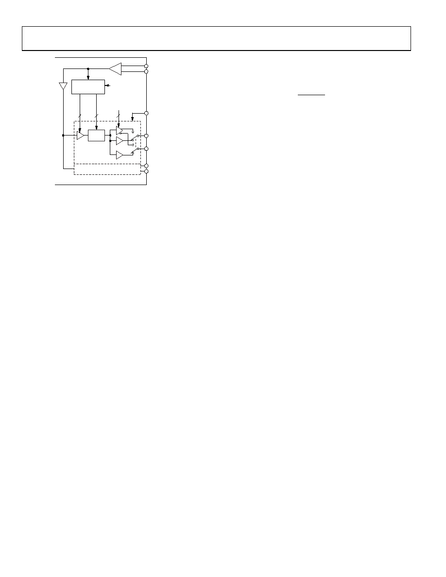
Q0
SYNC
CONTROL
ENABLEn/MODEn
SYNC SOURCE
CLKINP
OUT1P
OUT1N
OUT1
OUT0
CLKINN
OUT_RSET
OUT0P
OUT0N
RE
S
E
T
E
NABL
E
4
0
8300-
022
Figure 46. Clock Distribution
Clock Input (CLKINx)
The clock input handles input signals from a variety of logic
families (assuming proper terminations and sufficient voltage
swing). It also handles sine wave input signals such as those
delivered by the DAC reconstruction filter. Its default operating
frequency range is 62.5 MHz to 500 MHz.
Super-Nyquist Operation
Typically, the maximum usable frequency at the DAC output is
about 45% of the system clock frequency. However, because it is
a sampled DAC, its output spectrum contains Nyquist images.
Of particular interest are the images appearing in the first Nyquist
zone (50% to 100% of the system clock frequency). Super-Nyquist
operation takes advantage of these higher frequencies, but this
implies that the CLKINx input operates in excess of 500 MHz,
which is outside its default operating limits.
The CLKINx receiver actually consists of two separate receivers:
the default receiver and an optional high frequency receiver,
which handles input signals up to 800 MHz. To select the high
frequency receiver, write a Logic 1 to Register 0x0400, Bit4.
Super-Nyquist operation requires a band-pass filter at the DAC
output instead of the usual low-pass reconstruction filter. Super-
Nyquist operation is viable as long as the image frequency does
not exceed the 800 MHz input range of the receiver. Furthermore,
to provide acceptable jitter performance, which is a consideration
for image signals with low amplitude, the signal at the CLKINx
inputs must meet the minimum slew rate requirements.
Clock Dividers
The output clock distribution dividers are referred to as Q0 and Q1,
corresponding to the OUT0 and OUT1 output channels, respec-
tively. Each divider is programmable with 30 bits of division depth.
The actual divide ratio is one more than the programmed register
value; therefore, a register value of 3, for example, results in a
divide ratio of 4. Thus, each divider offers a range of divide ratios
from 1 to 230 (1 to 1,073,741,824).
With an even divide ratio, the output signal always exhibits a
50% duty cycle. When the clock divider is bypassed (a divide
ratio of 1), the output duty cycle is the same as the input duty
cycle. Odd output divide ratios (excluding 1) exhibit automatic
duty cycle correction given by
N
X
N
Cycle
Duty
Output
2
1
2
where:
N (which must be an odd number) is the divide ratio.
X is the normalized fraction of the high portion of the input period
(that is, 0 < X < 1).
For example, if N = 5 and the input duty cycle is 20% (X = 0.2),
then the output duty cycle is 44%. Note that, when the user
programs an output as noninverting, then the device adjusts the
falling edge timing to accomplish the duty cycle correction.
Conversely, the device adjusts the rising edge timing for an
inverted output.
Output Power-Down
Each output channel offers independent control of power-down
functionality via the distribution settings register (Address 0x0400).
Each output channel has a dedicated power-down bit for powering
down the output driver. However, if both channels are powered
down, the entire distribution output enters a deep sleep mode.
Even though each channel has a channel power-down control
signal, it may sometimes be desirable to power down an output
driver while maintaining the divider’s synchronization with the
other channel dividers. This is accomplished by either of the
following methods:
In CMOS mode, use the divider output enable control bit
to stall an output. This provides power savings while main-
taining dc drive at the output.
In LVDS/LVPECL mode, place the output in tristate mode
(this works in CMOS mode as well).
Output Enable
Each output channel offers independent control of enable/
disable functionality using the distribution enable register
(Address 0x0401). The distribution outputs use synchronization
logic to control enable/disable activity to avoid the production
of runt pulses and to ensure that outputs with the same divide
ratios become active/inactive in unison.
Output Mode
The user has independent control of the operating mode of each of
the two output channels via the distribution channel modes register
(Address 0x0404 and Address 0x0405). The operating mode
control includes
Logic family and pin functionality
Output drive strength
Output polarity
The three LSBs of both distribution channel mode registers com-
prise the mode bits. The mode value selects the desired logic family
and pin functionality of an output channel, as listed in Table 24.
相关PDF资料 |
PDF描述 |
|---|---|
| AD9548BCPZ-REEL7 | IC CLOCK GEN/SYNCHRONIZR 88LFCSP |
| AD9549ABCPZ-REEL7 | IC CLOCK GEN/SYNCHRONIZR 64LFCSP |
| AD9550BCPZ-REEL7 | IC INTEGER-N TRANSLATOR 32-LFCSP |
| AD9551BCPZ | IC CLOCK GEN MULTISERV 40-LFCSP |
| AD9552BCPZ-REEL7 | IC PLL CLOCK GEN LP 32LFCSP |
相关代理商/技术参数 |
参数描述 |
|---|---|
| AD9548 | 制造商:AD 制造商全称:Analog Devices 功能描述:Quad/Octal Input Network Clock Generator/Synchronizer |
| AD9548/PCBZ | 功能描述:BOARD EVAL FOR AD9548 RoHS:是 类别:编程器,开发系统 >> 评估演示板和套件 系列:- 标准包装:1 系列:PSoC® 主要目的:电源管理,热管理 嵌入式:- 已用 IC / 零件:- 主要属性:- 次要属性:- 已供物品:板,CD,电源 |
| AD9548/PCBZ | 制造商:Analog Devices 功能描述:Clock Generator Evaluation Board |
| AD9548BCPZ | 功能描述:IC CLOCK GEN/SYNCHRONIZR 88LFCSP RoHS:是 类别:集成电路 (IC) >> 时钟/计时 - 专用 系列:- 标准包装:1 系列:- 类型:时钟/频率发生器,多路复用器 PLL:是 主要目的:存储器,RDRAM 输入:晶体 输出:LVCMOS 电路数:1 比率 - 输入:输出:1:2 差分 - 输入:输出:无/是 频率 - 最大:400MHz 电源电压:3 V ~ 3.6 V 工作温度:0°C ~ 85°C 安装类型:表面贴装 封装/外壳:16-TSSOP(0.173",4.40mm 宽) 供应商设备封装:16-TSSOP 包装:Digi-Reel® 其它名称:296-6719-6 |
| AD9548BCPZ-REEL7 | 功能描述:IC CLOCK GEN/SYNCHRONIZR 88LFCSP RoHS:是 类别:集成电路 (IC) >> 时钟/计时 - 专用 系列:- 标准包装:28 系列:- 类型:时钟/频率发生器 PLL:是 主要目的:Intel CPU 服务器 输入:时钟 输出:LVCMOS 电路数:1 比率 - 输入:输出:3:22 差分 - 输入:输出:无/是 频率 - 最大:400MHz 电源电压:3.135 V ~ 3.465 V 工作温度:0°C ~ 85°C 安装类型:表面贴装 封装/外壳:64-TFSOP (0.240",6.10mm 宽) 供应商设备封装:64-TSSOP 包装:管件 |
发布紧急采购,3分钟左右您将得到回复。