- 您现在的位置:买卖IC网 > PDF目录1987 > AD9547BCPZ-REEL7 (Analog Devices Inc)IC CLOCK GEN/SYNCHRONIZR 64LFCSP PDF资料下载
参数资料
| 型号: | AD9547BCPZ-REEL7 |
| 厂商: | Analog Devices Inc |
| 文件页数: | 31/104页 |
| 文件大小: | 0K |
| 描述: | IC CLOCK GEN/SYNCHRONIZR 64LFCSP |
| 产品变化通告: | AD9547 Mask Change 20/Oct/2010 |
| 标准包装: | 750 |
| 类型: | 时钟/频率发生器,同步器 |
| PLL: | 是 |
| 主要目的: | 以太网,SONET/SDH,Stratum |
| 输入: | CMOS,LVDS,LVPECL |
| 输出: | CMOS,LVDS,LVPECL |
| 电路数: | 1 |
| 比率 - 输入:输出: | 2:2 |
| 差分 - 输入:输出: | 是/是 |
| 频率 - 最大: | 750kHz |
| 电源电压: | 1.71 V ~ 3.465 V |
| 工作温度: | -40°C ~ 85°C |
| 安装类型: | 表面贴装 |
| 封装/外壳: | 64-VFQFN 裸露焊盘,CSP |
| 供应商设备封装: | 64-LFCSP-VQ(9x9) |
| 包装: | 带卷 (TR) |
第1页第2页第3页第4页第5页第6页第7页第8页第9页第10页第11页第12页第13页第14页第15页第16页第17页第18页第19页第20页第21页第22页第23页第24页第25页第26页第27页第28页第29页第30页当前第31页第32页第33页第34页第35页第36页第37页第38页第39页第40页第41页第42页第43页第44页第45页第46页第47页第48页第49页第50页第51页第52页第53页第54页第55页第56页第57页第58页第59页第60页第61页第62页第63页第64页第65页第66页第67页第68页第69页第70页第71页第72页第73页第74页第75页第76页第77页第78页第79页第80页第81页第82页第83页第84页第85页第86页第87页第88页第89页第90页第91页第92页第93页第94页第95页第96页第97页第98页第99页第100页第101页第102页第103页第104页
AD9547
Data Sheet
Rev. E | Page 32 of 104
an increase in the phase slew rate limit value or a decrease in
the system clock frequency tends to reduce the error. Therefore,
the accuracy is best for the largest phase slew rate limit value and
the lowest system clock frequency. For example, assuming the
use of a 1 GHz system clock, a phase slew rate limit value of
315 ns/sec (or more) ensures an error of <10%, whereas a phase
slew rate limit value above ~3100 ns/sec ensures an error of <1%.
On the other hand, assuming the use of a 500 MHz system clock,
the same phase slew rate limit values ensure an error of <5% or
0.5%, respectively.
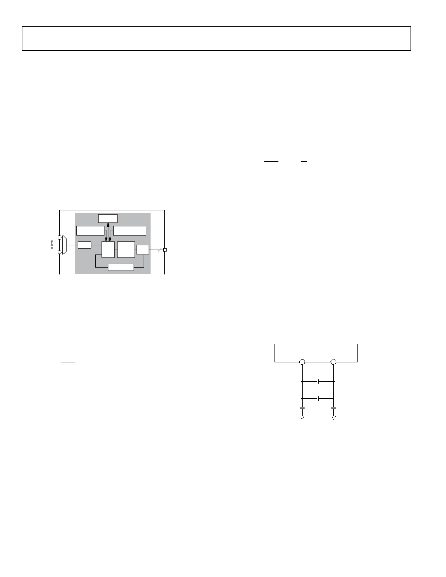
DIGITAL PHASE-LOCKED LOOP (DPLL) CORE
DPLL Overview
A diagram of the digital PLL core of the AD9547 appears in
Figure 36. The phase/frequency detector, feedback path, lock
detectors, phase offset, and phase slew rate limiting that make
up this second-generation DPLL are all digital implementations.
R + 1
REF A
TDC
AND
PFD
DIGITAL
LOOP
FILTER
DDS/
DAC
DACOUT
CLOSED-LOOP
PHASE OFFSET
PHASE SLEW
LIMIT
LOCK
DETECT
REF BB
DPPL CORE
2
fREF
fTDC
fDDS
S + 1 + U/V
08300-
0
13
Figure 36. Digital PLL Core
The start of the DPLL signal chain is the reference signal, fREF,
which is the frequency of the reference input. A reference
prescaler reduces the frequency of this signal by an integer
factor, R + 1, where R is the 30-bit value stored in the profile
register and 0 ≤ R ≤ 1,073,741,823. Therefore, the frequency at
the output of the R divider (or the input to the time-to-digital
converter (TDC)) is
1
R
f
REF
TDC
The TDC samples the output of the R divider. The TDC/PFD
produces a time series of digital words and delivers them to the
digital loop filter. The digital loop filter offers the following
advantages:
Determination of the filter response by numeric
coefficients rather than by discrete component values
Absence of analog components (R/L/C), which eliminates
tolerance variations due to aging
Absence of thermal noise associated with analog
components
Absence of control node leakage current associated with
analog components (a source of reference feed-through
spurs in the output spectrum of a traditional analog PLL)
The digital loop filter produces a time series of digital words
at its output and delivers them to the frequency tuning input of
a direct digital synthesizer (DDS), with the DDS replacing the
function of the VCO in an analog PLL. The digital words from
the loop filter tend to steer the DDS frequency toward frequency
and phase lock with the input signal (fTDC). The DDS provides
an analog output signal via an integrated DAC, effectively
mimicking the operation of an analog VCO.
The DPLL includes a feedback divider that causes the DDS to
operate at an integer-plus-fractional multiple (S + 1 + U/V) of
fTDC. S is the 20-bit value stored in the profile register and has a
range of 7 ≤ S ≤ 1,048,576. U and V are the 10-bit numerator
and denominator values of the optional fractional divide
component, also stored in the profile register. Together they
establish the nominal DDS frequency (fDDS), given by
V
U
S
R
f
REF
DDS
1
Normally, fractional-N designs exhibit distinctive phase noise
and spurious artifacts resulting from the modulation of the
integer divider based on the fractional value. This is not the
case for the AD9547 because it uses a purely digital means to
determine phase errors. Because the phase errors incurred by
modulating the feedback divider are deterministic, it is possible
to compensate for them digitally. The result is a fractional-N
PLL with no discernible modulation artifacts.
Time-to-Digital Converter (TDC)/Phase Frequency
Detector (PFD)
The TDC is a highly integrated functional block that incorporates
both analog and digital circuitry. There are two pins associated
with the TDC that the user must connect to external components.
Figure 37 shows the recommended component values and their
connections.
For best performance, place components as close as possible to
the device pins. Components with low effective series resistance
(ESR) and low parasitic inductance yield the best results.
AD9547
10F
0.1F
TDC_VRT
TDC_VRB
41
40
0830
0-
01
4
Figure 37. TDC Pin Connections
The PFD is an all-digital block. It compares the digital output from
the TDC (which relates to the active reference edge) with the
digital word from the feedback block (which relates to the roll-
over edge of the DDS accumulator after division by the feedback
divider). The PFD uses a digital code pump and digital integrator
(rather than a conventional charge pump and capacitor) to generate
the error signal that steers the DDS frequency toward phase lock.
Closed-Loop Phase Offset
The all-digital nature of the TDC/PFD provides for numerical
control of the phase offset between the reference and feedback
edges. This allows the user to adjust the relative timing of the
distribution output edges relative to the reference input edges by
相关PDF资料 |
PDF描述 |
|---|---|
| AD9548BCPZ-REEL7 | IC CLOCK GEN/SYNCHRONIZR 88LFCSP |
| AD9549ABCPZ-REEL7 | IC CLOCK GEN/SYNCHRONIZR 64LFCSP |
| AD9550BCPZ-REEL7 | IC INTEGER-N TRANSLATOR 32-LFCSP |
| AD9551BCPZ | IC CLOCK GEN MULTISERV 40-LFCSP |
| AD9552BCPZ-REEL7 | IC PLL CLOCK GEN LP 32LFCSP |
相关代理商/技术参数 |
参数描述 |
|---|---|
| AD9548 | 制造商:AD 制造商全称:Analog Devices 功能描述:Quad/Octal Input Network Clock Generator/Synchronizer |
| AD9548/PCBZ | 功能描述:BOARD EVAL FOR AD9548 RoHS:是 类别:编程器,开发系统 >> 评估演示板和套件 系列:- 标准包装:1 系列:PSoC® 主要目的:电源管理,热管理 嵌入式:- 已用 IC / 零件:- 主要属性:- 次要属性:- 已供物品:板,CD,电源 |
| AD9548/PCBZ | 制造商:Analog Devices 功能描述:Clock Generator Evaluation Board |
| AD9548BCPZ | 功能描述:IC CLOCK GEN/SYNCHRONIZR 88LFCSP RoHS:是 类别:集成电路 (IC) >> 时钟/计时 - 专用 系列:- 标准包装:1 系列:- 类型:时钟/频率发生器,多路复用器 PLL:是 主要目的:存储器,RDRAM 输入:晶体 输出:LVCMOS 电路数:1 比率 - 输入:输出:1:2 差分 - 输入:输出:无/是 频率 - 最大:400MHz 电源电压:3 V ~ 3.6 V 工作温度:0°C ~ 85°C 安装类型:表面贴装 封装/外壳:16-TSSOP(0.173",4.40mm 宽) 供应商设备封装:16-TSSOP 包装:Digi-Reel® 其它名称:296-6719-6 |
| AD9548BCPZ-REEL7 | 功能描述:IC CLOCK GEN/SYNCHRONIZR 88LFCSP RoHS:是 类别:集成电路 (IC) >> 时钟/计时 - 专用 系列:- 标准包装:28 系列:- 类型:时钟/频率发生器 PLL:是 主要目的:Intel CPU 服务器 输入:时钟 输出:LVCMOS 电路数:1 比率 - 输入:输出:3:22 差分 - 输入:输出:无/是 频率 - 最大:400MHz 电源电压:3.135 V ~ 3.465 V 工作温度:0°C ~ 85°C 安装类型:表面贴装 封装/外壳:64-TFSOP (0.240",6.10mm 宽) 供应商设备封装:64-TSSOP 包装:管件 |
发布紧急采购,3分钟左右您将得到回复。