- 您现在的位置:买卖IC网 > PDF目录1987 > AD9547BCPZ-REEL7 (Analog Devices Inc)IC CLOCK GEN/SYNCHRONIZR 64LFCSP PDF资料下载
参数资料
| 型号: | AD9547BCPZ-REEL7 |
| 厂商: | Analog Devices Inc |
| 文件页数: | 56/104页 |
| 文件大小: | 0K |
| 描述: | IC CLOCK GEN/SYNCHRONIZR 64LFCSP |
| 产品变化通告: | AD9547 Mask Change 20/Oct/2010 |
| 标准包装: | 750 |
| 类型: | 时钟/频率发生器,同步器 |
| PLL: | 是 |
| 主要目的: | 以太网,SONET/SDH,Stratum |
| 输入: | CMOS,LVDS,LVPECL |
| 输出: | CMOS,LVDS,LVPECL |
| 电路数: | 1 |
| 比率 - 输入:输出: | 2:2 |
| 差分 - 输入:输出: | 是/是 |
| 频率 - 最大: | 750kHz |
| 电源电压: | 1.71 V ~ 3.465 V |
| 工作温度: | -40°C ~ 85°C |
| 安装类型: | 表面贴装 |
| 封装/外壳: | 64-VFQFN 裸露焊盘,CSP |
| 供应商设备封装: | 64-LFCSP-VQ(9x9) |
| 包装: | 带卷 (TR) |
第1页第2页第3页第4页第5页第6页第7页第8页第9页第10页第11页第12页第13页第14页第15页第16页第17页第18页第19页第20页第21页第22页第23页第24页第25页第26页第27页第28页第29页第30页第31页第32页第33页第34页第35页第36页第37页第38页第39页第40页第41页第42页第43页第44页第45页第46页第47页第48页第49页第50页第51页第52页第53页第54页第55页当前第56页第57页第58页第59页第60页第61页第62页第63页第64页第65页第66页第67页第68页第69页第70页第71页第72页第73页第74页第75页第76页第77页第78页第79页第80页第81页第82页第83页第84页第85页第86页第87页第88页第89页第90页第91页第92页第93页第94页第95页第96页第97页第98页第99页第100页第101页第102页第103页第104页
Data Sheet
AD9547
Rev. E | Page 55 of 104
IC SERIAL PORT OPERATION
The I2C interface has the advantage of requiring only two
control pins and is a de facto standard throughout the I2C
industry. However, its disadvantage is programming speed,
which is 400 kbps maximum. The AD9547 I2C port design is
based on the I2C fast mode standard from Philips, so it supports
both the 100 kHz standard mode and the 400 kHz fast mode.
Fast mode imposes a glitch tolerance requirement on the control
signals; that is, the input receivers ignore pulses of less than
50 ns duration.
The AD9547 I2C port consists of a serial data line (SDA) and
a serial clock line (SCL). In an I2C bus system, the AD9547 is
connected to the serial bus (data bus SDA and clock bus SCL)
as a slave device; that is, no clock is generated by the AD9547.
The AD9547 uses direct 16-bit memory addressing instead of
traditional 8-bit memory addressing.
The AD9547 allows for up to seven unique slave devices to occupy
the I2C bus. These are accessed via a 7-bit slave address that is
transmitted as part of an I2C packet. Only the device with a match-
ing slave address responds to subsequent I2C commands. The
device slave address is 1001xxx (the last three bits are determined
by the M0 to M2 pins). The four MSBs (1001) are hardwired,
whereas the three LSBs (xxx, determined by the M0 to M2 pins)
are programmable via the power-up state of the multifunction
pins (see the Initial M0 to M7 Pin Programming section).
I2C Bus Characteristics
Table 35. I2C Bus Abbreviation Definitions
Abbreviation
Definition
S
Start
Sr
Repeated start
P
Stop
A
Acknowledge
A
No acknowledge
W
Write
R
Read
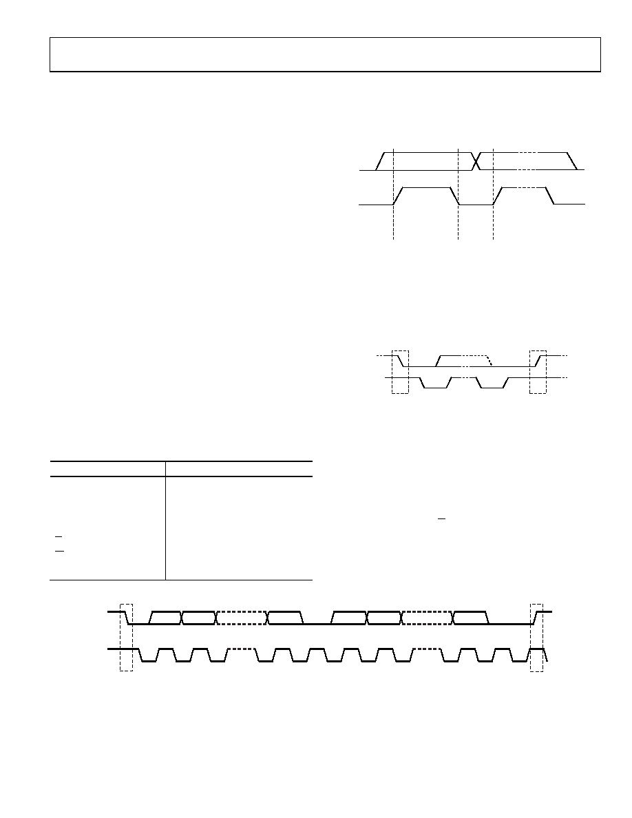
The transfer of data appears graphically in Figure 59. One clock
pulse is generated for each data bit transferred. The data on the
SDA line must be stable during the high period of the clock.
The high or low state of the data line can change only when the
clock signal on the SCL line is low.
DATA LINE
STABLE;
DATA VALID
CHANGE
OF DATA
ALLOWED
SDA
SCL
08300-
035
Figure 59. Valid Bit Transfer
Start/stop functionality appears graphically in Figure 60. The
start condition is characterized by a high-to-low transition on
the SDA line while SCL is high. The start condition is always
generated by the master to initialize data transfer. The stop
condition is characterized by a low-to-high transition on the
SDA line while SCL is high. The stop condition is always
generated by the master to terminate data transfer.
SDA
START CONDITION
STOP CONDITION
SCL
SP
08300-
036
Figure 60. Start and Stop Condition
Every byte on the SDA line must be eight bits long. Each byte
must be followed by an acknowledge bit. Bytes are sent MSB first.
The acknowledge bit (A) is the ninth bit attached to any 8-bit
data byte. An acknowledge bit is always generated by the
receiving device (receiver) to inform the transmitter that the
byte has been received. It is done by pulling the SDA line low
during the ninth clock pulse after each 8-bit data byte.
The no acknowledge bit (A) is the ninth bit attached to any 8-bit
data byte. A no acknowledge bit is always generated by the
receiving device (receiver) to inform the transmitter that the
byte has not been received. It is done by leaving the SDA line
high during the ninth clock pulse after each 8-bit data byte.
12
89
12
3 TO 7
89
10
SDA
SCL
S
MSB
ACK FROM
SLAVE RECEIVER
ACK FROM
SLAVE RECEIVER
P
08
30
0-
03
7
Figure 61. Acknowledge Bit
相关PDF资料 |
PDF描述 |
|---|---|
| AD9548BCPZ-REEL7 | IC CLOCK GEN/SYNCHRONIZR 88LFCSP |
| AD9549ABCPZ-REEL7 | IC CLOCK GEN/SYNCHRONIZR 64LFCSP |
| AD9550BCPZ-REEL7 | IC INTEGER-N TRANSLATOR 32-LFCSP |
| AD9551BCPZ | IC CLOCK GEN MULTISERV 40-LFCSP |
| AD9552BCPZ-REEL7 | IC PLL CLOCK GEN LP 32LFCSP |
相关代理商/技术参数 |
参数描述 |
|---|---|
| AD9548 | 制造商:AD 制造商全称:Analog Devices 功能描述:Quad/Octal Input Network Clock Generator/Synchronizer |
| AD9548/PCBZ | 功能描述:BOARD EVAL FOR AD9548 RoHS:是 类别:编程器,开发系统 >> 评估演示板和套件 系列:- 标准包装:1 系列:PSoC® 主要目的:电源管理,热管理 嵌入式:- 已用 IC / 零件:- 主要属性:- 次要属性:- 已供物品:板,CD,电源 |
| AD9548/PCBZ | 制造商:Analog Devices 功能描述:Clock Generator Evaluation Board |
| AD9548BCPZ | 功能描述:IC CLOCK GEN/SYNCHRONIZR 88LFCSP RoHS:是 类别:集成电路 (IC) >> 时钟/计时 - 专用 系列:- 标准包装:1 系列:- 类型:时钟/频率发生器,多路复用器 PLL:是 主要目的:存储器,RDRAM 输入:晶体 输出:LVCMOS 电路数:1 比率 - 输入:输出:1:2 差分 - 输入:输出:无/是 频率 - 最大:400MHz 电源电压:3 V ~ 3.6 V 工作温度:0°C ~ 85°C 安装类型:表面贴装 封装/外壳:16-TSSOP(0.173",4.40mm 宽) 供应商设备封装:16-TSSOP 包装:Digi-Reel® 其它名称:296-6719-6 |
| AD9548BCPZ-REEL7 | 功能描述:IC CLOCK GEN/SYNCHRONIZR 88LFCSP RoHS:是 类别:集成电路 (IC) >> 时钟/计时 - 专用 系列:- 标准包装:28 系列:- 类型:时钟/频率发生器 PLL:是 主要目的:Intel CPU 服务器 输入:时钟 输出:LVCMOS 电路数:1 比率 - 输入:输出:3:22 差分 - 输入:输出:无/是 频率 - 最大:400MHz 电源电压:3.135 V ~ 3.465 V 工作温度:0°C ~ 85°C 安装类型:表面贴装 封装/外壳:64-TFSOP (0.240",6.10mm 宽) 供应商设备封装:64-TSSOP 包装:管件 |
发布紧急采购,3分钟左右您将得到回复。