- 您现在的位置:买卖IC网 > PDF目录1987 > AD9547BCPZ-REEL7 (Analog Devices Inc)IC CLOCK GEN/SYNCHRONIZR 64LFCSP PDF资料下载
参数资料
| 型号: | AD9547BCPZ-REEL7 |
| 厂商: | Analog Devices Inc |
| 文件页数: | 53/104页 |
| 文件大小: | 0K |
| 描述: | IC CLOCK GEN/SYNCHRONIZR 64LFCSP |
| 产品变化通告: | AD9547 Mask Change 20/Oct/2010 |
| 标准包装: | 750 |
| 类型: | 时钟/频率发生器,同步器 |
| PLL: | 是 |
| 主要目的: | 以太网,SONET/SDH,Stratum |
| 输入: | CMOS,LVDS,LVPECL |
| 输出: | CMOS,LVDS,LVPECL |
| 电路数: | 1 |
| 比率 - 输入:输出: | 2:2 |
| 差分 - 输入:输出: | 是/是 |
| 频率 - 最大: | 750kHz |
| 电源电压: | 1.71 V ~ 3.465 V |
| 工作温度: | -40°C ~ 85°C |
| 安装类型: | 表面贴装 |
| 封装/外壳: | 64-VFQFN 裸露焊盘,CSP |
| 供应商设备封装: | 64-LFCSP-VQ(9x9) |
| 包装: | 带卷 (TR) |
第1页第2页第3页第4页第5页第6页第7页第8页第9页第10页第11页第12页第13页第14页第15页第16页第17页第18页第19页第20页第21页第22页第23页第24页第25页第26页第27页第28页第29页第30页第31页第32页第33页第34页第35页第36页第37页第38页第39页第40页第41页第42页第43页第44页第45页第46页第47页第48页第49页第50页第51页第52页当前第53页第54页第55页第56页第57页第58页第59页第60页第61页第62页第63页第64页第65页第66页第67页第68页第69页第70页第71页第72页第73页第74页第75页第76页第77页第78页第79页第80页第81页第82页第83页第84页第85页第86页第87页第88页第89页第90页第91页第92页第93页第94页第95页第96页第97页第98页第99页第100页第101页第102页第103页第104页
AD9547
Data Sheet
Rev. E | Page 52 of 104
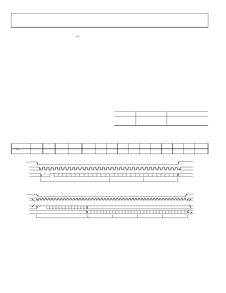
SPI Instruction Word (16 Bits)
The MSB of the 16-bit instruction word is R/W, which indicates
whether the instruction is a read or a write. The next two bits, W1
and W0, indicate the number of bytes in the transfer (see Table 31).
The final 13 bits are the register address (A12 to A0), which indi-
cates the starting register address of the read/write operation
(see Table 33).
SPI MSB/LSB First Transfers
The AD9547 instruction word and payload can be MSB first or
LSB first. The default for the AD9547 is MSB first. The LSB-first
mode can be set by writing a 1 to Register 0x0000, Bit 6. Immedi-
ately after the LSB-first bit is set, subsequent serial control port
operations are LSB first.
When MSB-first mode is active, the instruction and data bytes
must be written from MSB to LSB. Multibyte data transfers in
MSB-first format start with an instruction byte that includes the
register address of the most significant payload byte. Subsequent
data bytes must follow in order from high address to low address.
In MSB-first mode, the serial control port internal address
generator decrements for each data byte of the multibyte
transfer cycle.
When Register 0x0000, Bit 6 = 1 (LSB first), the instruction and
data bytes must be written from LSB to MSB. Multibyte data trans-
fers in LSB-first format start with an instruction byte that includes
the register address of the least significant payload byte, followed
by multiple data bytes. The serial control port internal byte address
generator increments for each byte of the multibyte transfer cycle.
For multibyte MSB-first (default) I/O operations, the serial control
port register address decrements from the specified starting address
toward Address 0x0000. For multibyte LSB-first I/O operations,
the serial control port register address increments from the starting
address toward Address 0x1FFF. Unused addresses are not skipped
during multibyte I/O operations; therefore, the user should
write the default value to a reserved register and 0s to unmapped
registers. Note that it is more efficient to issue a new write
command than to write the default value to more than two
consecutive reserved (or unmapped) registers.
Table 32. Streaming Mode (No Addresses Are Skipped)
Write Mode
Address Direction
Stop Sequence
LSB First
Increment
0x0000 ... 0x1FFF
MSB First
Decrement
0x1FFF ... 0x0000
Table 33. Serial Control Port, 16-Bit Instruction Word, MSB First
MSB
LSB
I15
I14
I13
I12
I11
I10
I9
I8
I7
I6
I5
I4
I3
I2
I1
I0
R/W
W1
W0
A12
A11
A10
A9
A8
A7
A6
A5
A4
A3
A2
A1
A0
CS
SCLK DON'T CARE
SDIO
A12
W0
W1
R/W
A11 A10 A9
A8
A7
A6
A5
A4
A3
A2
A1
A0
D7 D6
D5
D4
D3
D2 D1
D0
D7
D6
D5
D4
D3
D2
D1
D0
DON'T CARE
16-BIT INSTRUCTION HEADER
REGISTER (N) DATA
REGISTER (N – 1) DATA
0
8300
-02
9
Figure 52. Serial Control Port Write—MSB First, 16-Bit Instruction, Two Bytes of Data
CS
SCLK
SDIO
SDO
REGISTER (N) DATA
16-BIT INSTRUCTION HEADER
REGISTER (N – 1) DATA
REGISTER (N – 2) DATA
REGISTER (N – 3) DATA
A12
W0
W1
R/W
A11 A10 A9 A8 A7 A6 A5 A4 A3 A2 A1 A0
DON'T CARE
DON'T
CARE
D7 D6 D5 D4 D3 D2 D1 D0 D7 D6 D5 D4 D3 D2 D1 D0 D7 D6 D5 D4 D3 D2 D1 D0 D7 D6 D5 D4 D3 D2 D1 D0
08
300-
030
Figure 53. Serial Control Port Read—MSB First, 16-Bit Instruction, Four Bytes of Data
相关PDF资料 |
PDF描述 |
|---|---|
| AD9548BCPZ-REEL7 | IC CLOCK GEN/SYNCHRONIZR 88LFCSP |
| AD9549ABCPZ-REEL7 | IC CLOCK GEN/SYNCHRONIZR 64LFCSP |
| AD9550BCPZ-REEL7 | IC INTEGER-N TRANSLATOR 32-LFCSP |
| AD9551BCPZ | IC CLOCK GEN MULTISERV 40-LFCSP |
| AD9552BCPZ-REEL7 | IC PLL CLOCK GEN LP 32LFCSP |
相关代理商/技术参数 |
参数描述 |
|---|---|
| AD9548 | 制造商:AD 制造商全称:Analog Devices 功能描述:Quad/Octal Input Network Clock Generator/Synchronizer |
| AD9548/PCBZ | 功能描述:BOARD EVAL FOR AD9548 RoHS:是 类别:编程器,开发系统 >> 评估演示板和套件 系列:- 标准包装:1 系列:PSoC® 主要目的:电源管理,热管理 嵌入式:- 已用 IC / 零件:- 主要属性:- 次要属性:- 已供物品:板,CD,电源 |
| AD9548/PCBZ | 制造商:Analog Devices 功能描述:Clock Generator Evaluation Board |
| AD9548BCPZ | 功能描述:IC CLOCK GEN/SYNCHRONIZR 88LFCSP RoHS:是 类别:集成电路 (IC) >> 时钟/计时 - 专用 系列:- 标准包装:1 系列:- 类型:时钟/频率发生器,多路复用器 PLL:是 主要目的:存储器,RDRAM 输入:晶体 输出:LVCMOS 电路数:1 比率 - 输入:输出:1:2 差分 - 输入:输出:无/是 频率 - 最大:400MHz 电源电压:3 V ~ 3.6 V 工作温度:0°C ~ 85°C 安装类型:表面贴装 封装/外壳:16-TSSOP(0.173",4.40mm 宽) 供应商设备封装:16-TSSOP 包装:Digi-Reel® 其它名称:296-6719-6 |
| AD9548BCPZ-REEL7 | 功能描述:IC CLOCK GEN/SYNCHRONIZR 88LFCSP RoHS:是 类别:集成电路 (IC) >> 时钟/计时 - 专用 系列:- 标准包装:28 系列:- 类型:时钟/频率发生器 PLL:是 主要目的:Intel CPU 服务器 输入:时钟 输出:LVCMOS 电路数:1 比率 - 输入:输出:3:22 差分 - 输入:输出:无/是 频率 - 最大:400MHz 电源电压:3.135 V ~ 3.465 V 工作温度:0°C ~ 85°C 安装类型:表面贴装 封装/外壳:64-TFSOP (0.240",6.10mm 宽) 供应商设备封装:64-TSSOP 包装:管件 |
发布紧急采购,3分钟左右您将得到回复。