- 您现在的位置:买卖IC网 > PDF目录1987 > AD9547BCPZ-REEL7 (Analog Devices Inc)IC CLOCK GEN/SYNCHRONIZR 64LFCSP PDF资料下载
参数资料
| 型号: | AD9547BCPZ-REEL7 |
| 厂商: | Analog Devices Inc |
| 文件页数: | 57/104页 |
| 文件大小: | 0K |
| 描述: | IC CLOCK GEN/SYNCHRONIZR 64LFCSP |
| 产品变化通告: | AD9547 Mask Change 20/Oct/2010 |
| 标准包装: | 750 |
| 类型: | 时钟/频率发生器,同步器 |
| PLL: | 是 |
| 主要目的: | 以太网,SONET/SDH,Stratum |
| 输入: | CMOS,LVDS,LVPECL |
| 输出: | CMOS,LVDS,LVPECL |
| 电路数: | 1 |
| 比率 - 输入:输出: | 2:2 |
| 差分 - 输入:输出: | 是/是 |
| 频率 - 最大: | 750kHz |
| 电源电压: | 1.71 V ~ 3.465 V |
| 工作温度: | -40°C ~ 85°C |
| 安装类型: | 表面贴装 |
| 封装/外壳: | 64-VFQFN 裸露焊盘,CSP |
| 供应商设备封装: | 64-LFCSP-VQ(9x9) |
| 包装: | 带卷 (TR) |
第1页第2页第3页第4页第5页第6页第7页第8页第9页第10页第11页第12页第13页第14页第15页第16页第17页第18页第19页第20页第21页第22页第23页第24页第25页第26页第27页第28页第29页第30页第31页第32页第33页第34页第35页第36页第37页第38页第39页第40页第41页第42页第43页第44页第45页第46页第47页第48页第49页第50页第51页第52页第53页第54页第55页第56页当前第57页第58页第59页第60页第61页第62页第63页第64页第65页第66页第67页第68页第69页第70页第71页第72页第73页第74页第75页第76页第77页第78页第79页第80页第81页第82页第83页第84页第85页第86页第87页第88页第89页第90页第91页第92页第93页第94页第95页第96页第97页第98页第99页第100页第101页第102页第103页第104页
AD9547
Data Sheet
Rev. E | Page 56 of 104
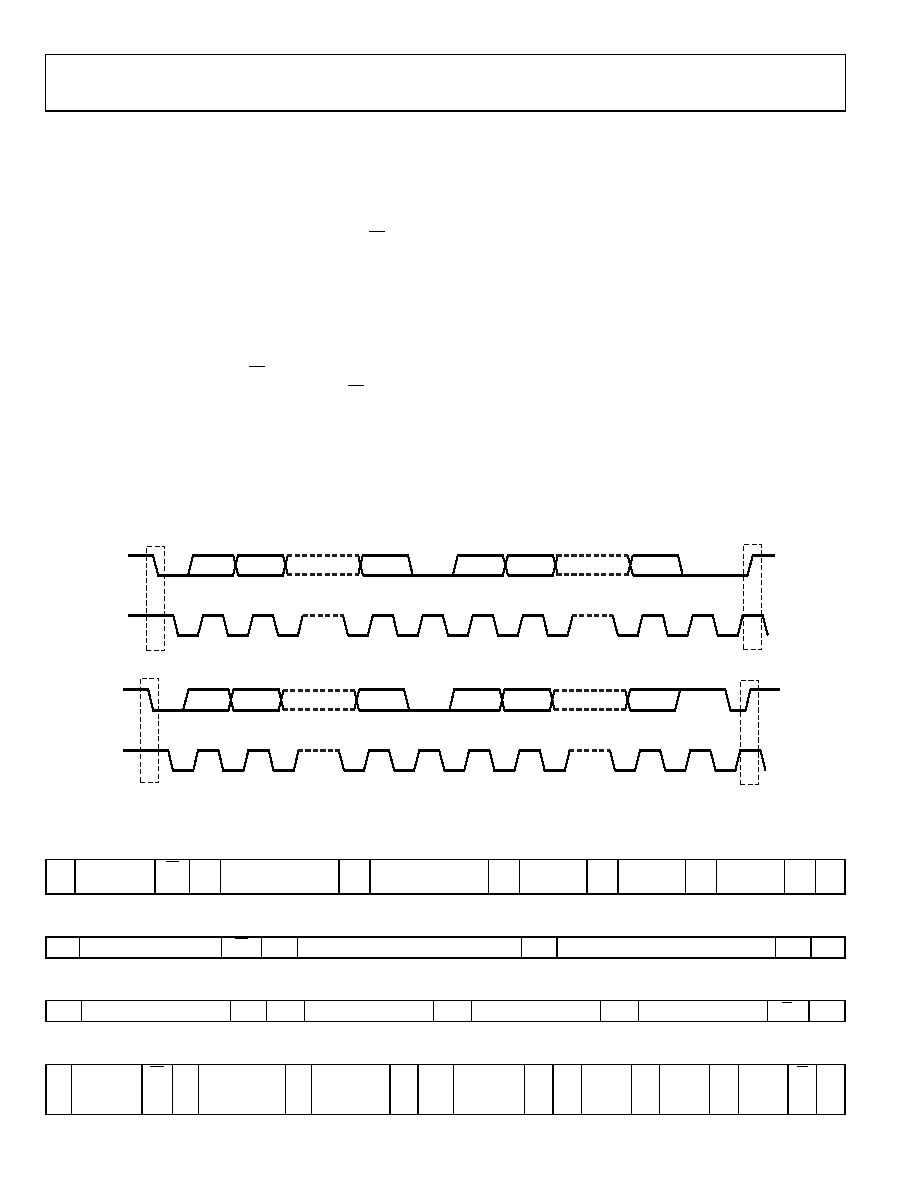
Data Transfer Process
The master initiates data transfer by asserting a start condition.
This indicates that a data stream follows. All I2C slave devices
connected to the serial bus respond to the start condition.
The master then sends an 8-bit address byte over the SDA line,
consisting of a 7-bit slave address (MSB first) plus an R/W bit.
This bit determines the direction of the data transfer, that is,
whether data is written to or read from the slave device (0 =
write, 1 = read).
The peripheral whose address corresponds to the transmitted
address responds by sending an acknowledge bit. All other devices
on the bus remain idle while the selected device waits for data to be
read from or written to it. If the R/W bit = 0, the master (trans-
mitter) writes to the slave device (receiver). If the R/W bit = 1,
the master (receiver) reads from the slave device (transmitter).
See the Data Transfer Format section for the command format.
Data is then sent over the serial bus in the format of nine clock
pulses, one data byte (eight bits) from either master (write mode)
or slave (read mode) followed by an acknowledge bit from the
receiving device. The number of bytes that can be transmitted
per transfer is unrestricted. In write mode, the first two data
bytes immediately after the slave address byte are the internal
memory (control registers) address bytes with the high address
byte first. This addressing scheme gives a memory address up to
216 1 = 65,535. The data bytes after these two memory address
bytes are register data written into or read from the control regi-
sters. In read mode, the data bytes after the slave address byte are
register data written into or read from the control registers.
When all data bytes are read or written, stop conditions are estab-
lished. In write mode, the master (transmitter) asserts a stop
condition to end data transfer during the 10th clock pulse following
the acknowledge bit for the last data byte from the slave device
(receiver). In read mode, the master device (receiver) receives the
last data byte from the slave device (transmitter) but does not pull
SDA low during the ninth clock pulse. This is known as a no
acknowledge bit. When receiving the no acknowledge bit, the slave
device knows the data transfer is finished and enters idle mode.
The master then takes the data line low during the low period
before the 10th clock pulse, and high during the 10th clock pulse
to assert a stop condition.
A start condition can be used in place of a stop condition.
Furthermore, a start or stop condition can occur at any time,
and partially transferred bytes are discarded.
12
89
12
3 TO 7
89
10
ACK FROM
SLAVE RECEIVER
ACK FROM
SLAVE RECEIVER
SDA
SCL
S
MSB
P
08
30
0-
0
38
Figure 62. Data Transfer Process (Master Write Mode, 2-Byte Transfer Used for Illustration)
12
89
12
3 TO 7
89
10
ACK FROM
MASTER RECEIVER
NO ACK FROM
MASTER RECEIVER
SDA
SCL
S
P
08
30
0-
03
9
Figure 63. Data Transfer Process (Master Read Mode, 2-Byte Transfer Used for Illustration)
Data Transfer Format
In write byte format, the write byte protocol is used to write a register address to the RAM starting from the specified RAM address.
S
Slave
Address
W
A
RAM Address
High Byte
A
RAM Address
Low Byte
A
RAM
Data 0
A
RAM
Data 1
A
RAM
Data 2
A
P
In send byte format, the send byte protocol is used to set up the register address for subsequent reads.
S
Slave Address
W
A
RAM Address High Byte
A
RAM Address Low Byte
A
P
In receive byte format, the receive byte protocol is used to read the data bytes from RAM starting from the current address.
S
Slave Address
R
A
RAM Data 0
A
RAM Data 1
A
RAM Data 2
A
P
Read byte format combines the format of the send byte and the receive byte formats.
S
Slave
Address
W
A
RAM
Address
High Byte
A
RAM
Address
Low Byte
A
Sr
Slave
Address
R
A
RAM
Data
0
A
RAM
Data
1
A
RAM
Data
2
A
P
相关PDF资料 |
PDF描述 |
|---|---|
| AD9548BCPZ-REEL7 | IC CLOCK GEN/SYNCHRONIZR 88LFCSP |
| AD9549ABCPZ-REEL7 | IC CLOCK GEN/SYNCHRONIZR 64LFCSP |
| AD9550BCPZ-REEL7 | IC INTEGER-N TRANSLATOR 32-LFCSP |
| AD9551BCPZ | IC CLOCK GEN MULTISERV 40-LFCSP |
| AD9552BCPZ-REEL7 | IC PLL CLOCK GEN LP 32LFCSP |
相关代理商/技术参数 |
参数描述 |
|---|---|
| AD9548 | 制造商:AD 制造商全称:Analog Devices 功能描述:Quad/Octal Input Network Clock Generator/Synchronizer |
| AD9548/PCBZ | 功能描述:BOARD EVAL FOR AD9548 RoHS:是 类别:编程器,开发系统 >> 评估演示板和套件 系列:- 标准包装:1 系列:PSoC® 主要目的:电源管理,热管理 嵌入式:- 已用 IC / 零件:- 主要属性:- 次要属性:- 已供物品:板,CD,电源 |
| AD9548/PCBZ | 制造商:Analog Devices 功能描述:Clock Generator Evaluation Board |
| AD9548BCPZ | 功能描述:IC CLOCK GEN/SYNCHRONIZR 88LFCSP RoHS:是 类别:集成电路 (IC) >> 时钟/计时 - 专用 系列:- 标准包装:1 系列:- 类型:时钟/频率发生器,多路复用器 PLL:是 主要目的:存储器,RDRAM 输入:晶体 输出:LVCMOS 电路数:1 比率 - 输入:输出:1:2 差分 - 输入:输出:无/是 频率 - 最大:400MHz 电源电压:3 V ~ 3.6 V 工作温度:0°C ~ 85°C 安装类型:表面贴装 封装/外壳:16-TSSOP(0.173",4.40mm 宽) 供应商设备封装:16-TSSOP 包装:Digi-Reel® 其它名称:296-6719-6 |
| AD9548BCPZ-REEL7 | 功能描述:IC CLOCK GEN/SYNCHRONIZR 88LFCSP RoHS:是 类别:集成电路 (IC) >> 时钟/计时 - 专用 系列:- 标准包装:28 系列:- 类型:时钟/频率发生器 PLL:是 主要目的:Intel CPU 服务器 输入:时钟 输出:LVCMOS 电路数:1 比率 - 输入:输出:3:22 差分 - 输入:输出:无/是 频率 - 最大:400MHz 电源电压:3.135 V ~ 3.465 V 工作温度:0°C ~ 85°C 安装类型:表面贴装 封装/外壳:64-TFSOP (0.240",6.10mm 宽) 供应商设备封装:64-TSSOP 包装:管件 |
发布紧急采购,3分钟左右您将得到回复。