- 您现在的位置:买卖IC网 > PDF目录1987 > AD9547BCPZ-REEL7 (Analog Devices Inc)IC CLOCK GEN/SYNCHRONIZR 64LFCSP PDF资料下载
参数资料
| 型号: | AD9547BCPZ-REEL7 |
| 厂商: | Analog Devices Inc |
| 文件页数: | 42/104页 |
| 文件大小: | 0K |
| 描述: | IC CLOCK GEN/SYNCHRONIZR 64LFCSP |
| 产品变化通告: | AD9547 Mask Change 20/Oct/2010 |
| 标准包装: | 750 |
| 类型: | 时钟/频率发生器,同步器 |
| PLL: | 是 |
| 主要目的: | 以太网,SONET/SDH,Stratum |
| 输入: | CMOS,LVDS,LVPECL |
| 输出: | CMOS,LVDS,LVPECL |
| 电路数: | 1 |
| 比率 - 输入:输出: | 2:2 |
| 差分 - 输入:输出: | 是/是 |
| 频率 - 最大: | 750kHz |
| 电源电压: | 1.71 V ~ 3.465 V |
| 工作温度: | -40°C ~ 85°C |
| 安装类型: | 表面贴装 |
| 封装/外壳: | 64-VFQFN 裸露焊盘,CSP |
| 供应商设备封装: | 64-LFCSP-VQ(9x9) |
| 包装: | 带卷 (TR) |
第1页第2页第3页第4页第5页第6页第7页第8页第9页第10页第11页第12页第13页第14页第15页第16页第17页第18页第19页第20页第21页第22页第23页第24页第25页第26页第27页第28页第29页第30页第31页第32页第33页第34页第35页第36页第37页第38页第39页第40页第41页当前第42页第43页第44页第45页第46页第47页第48页第49页第50页第51页第52页第53页第54页第55页第56页第57页第58页第59页第60页第61页第62页第63页第64页第65页第66页第67页第68页第69页第70页第71页第72页第73页第74页第75页第76页第77页第78页第79页第80页第81页第82页第83页第84页第85页第86页第87页第88页第89页第90页第91页第92页第93页第94页第95页第96页第97页第98页第99页第100页第101页第102页第103页第104页
AD9547
Data Sheet
Rev. E | Page 42 of 104
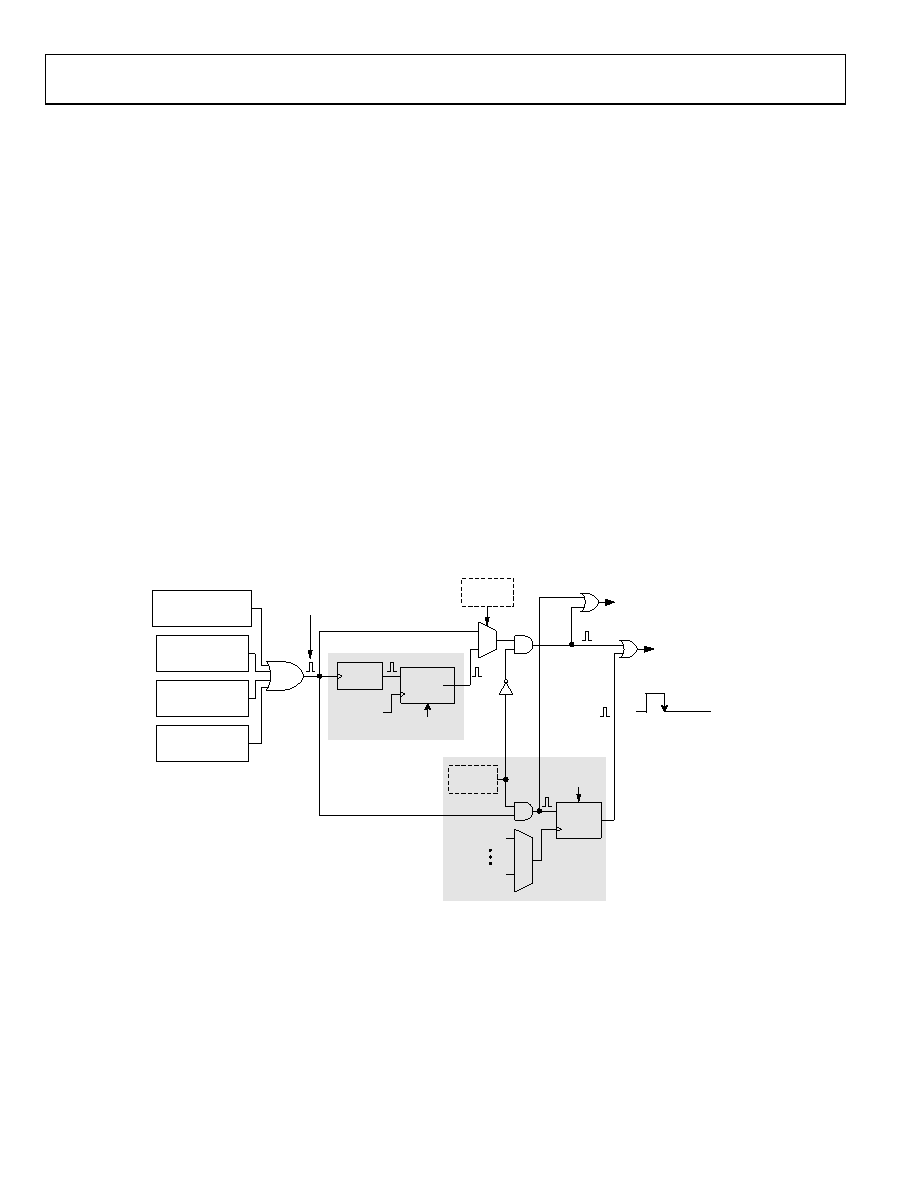
active input reference. The detection of the rising edge synchro-
nizes the distribution output.
When sync source = 10, the rising edge of the primary synchro-
nization signal triggers the circuitry that detects a rollover of the
DDS accumulator (after processing by the DPLL feedback divider).
This corresponds to the zero crossing of the output of the phase-to-
amplitude converter in the DDS (less the open-loop phase offset
stored in Register 0x030D and Register 0x030E). The detection
of the DPLL feedback edge synchronizes the distribution output.
Active Reference Synchronization (Zero Delay)
Active reference synchronization is the term applied to the case
when sync source = 01 (Register 0x0402, Bits[5:4]). Referring to
Figure 47, this means that the active reference sync path is active
because Bit 4 = 1, enabling the lower AND gate and disabling
the upper AND gate. The edge detector in the active reference
sync block monitors the rising edges of the active reference
(the mux selects the active reference automatically). The edge
detector is armed via the primary synchronization signal, which
is one of the four inputs to the OR gate (typically the direct sync
source). As soon as the edge detector is armed, its output goes high,
which stalls the output dividers in the clock distribution block.
Furthermore, once armed, a rising edge from the active reference
forces the output of the edge detector low. This restarts the output
dividers, thereby synchronizing the clock distribution block.
The term zero delay applies because it provides a means to edge-
align the output signal with the active input reference signal.
Typically, zero-delay architectures use the output signal in the
feedback loop of a PLL to track input/output edge alignment.
Active reference synchronization, however, operates open loop.
That is, synchronization of the output via the distribution
synchronization logic occurs on a single edge of the active
reference.
The fact that an active reference edge triggers the falling edge of
the synchronization pulse means that the falling edge is asynchro-
nous to the signal that clocks the distribution output dividers
(CLKINx). Therefore, the output clock distribution logic reclocks
the internal synchronization pulse to synchronize it with the
CLKINx signal. This means that the output dividers restart after
a deterministic delay associated with the reclocking circuitry.
This deterministic delay has two components. The first deter-
ministic delay component is four or five periods of the CLKINx
signal. The one period uncertainty is due to the unknown position
of the asynchronous reference clock edge relative to the CLKINx
signal. The second deterministic delay component is one output
period of the distribution divider.
MULTIFUNCTION PIN
SYNC SOURCE
0
1
REGISTER
0x0402[5]
SYSCLK/4
DPLL
FEEDBACK
EDGE
REGISTER
0x0402[4]
REF A
REF BB
RESET
EDGE
DETECT
EDGE
DETECT
ARM
EDGE
DETECT
ARM
DIRECT SYNC
DPLL EDGE SYNC
ACTIVE REFERENCE SYNC
EEPROM SYNC
SOURCE
PRIMARY
SYNCHRONIZATION
SIGNAL
DIRECT SYNC
SOURCE
(ADDRESS DX 0x0A02[1])
AUTOMATIC SYNC
SOURCE
(REGISTER DX 0x0403)
TO CLOCK
DISTRIBUTION
SYNCHRONIZATION
CONTROL
STALL
DIVIDERS
SYNC OUTPUT
DISTRIBUTION
TO MULTIFUNCTION
PIN STATUS LOGIC
08
300-
02
3
Figure 47. Output Synchronization Block Diagram
相关PDF资料 |
PDF描述 |
|---|---|
| AD9548BCPZ-REEL7 | IC CLOCK GEN/SYNCHRONIZR 88LFCSP |
| AD9549ABCPZ-REEL7 | IC CLOCK GEN/SYNCHRONIZR 64LFCSP |
| AD9550BCPZ-REEL7 | IC INTEGER-N TRANSLATOR 32-LFCSP |
| AD9551BCPZ | IC CLOCK GEN MULTISERV 40-LFCSP |
| AD9552BCPZ-REEL7 | IC PLL CLOCK GEN LP 32LFCSP |
相关代理商/技术参数 |
参数描述 |
|---|---|
| AD9548 | 制造商:AD 制造商全称:Analog Devices 功能描述:Quad/Octal Input Network Clock Generator/Synchronizer |
| AD9548/PCBZ | 功能描述:BOARD EVAL FOR AD9548 RoHS:是 类别:编程器,开发系统 >> 评估演示板和套件 系列:- 标准包装:1 系列:PSoC® 主要目的:电源管理,热管理 嵌入式:- 已用 IC / 零件:- 主要属性:- 次要属性:- 已供物品:板,CD,电源 |
| AD9548/PCBZ | 制造商:Analog Devices 功能描述:Clock Generator Evaluation Board |
| AD9548BCPZ | 功能描述:IC CLOCK GEN/SYNCHRONIZR 88LFCSP RoHS:是 类别:集成电路 (IC) >> 时钟/计时 - 专用 系列:- 标准包装:1 系列:- 类型:时钟/频率发生器,多路复用器 PLL:是 主要目的:存储器,RDRAM 输入:晶体 输出:LVCMOS 电路数:1 比率 - 输入:输出:1:2 差分 - 输入:输出:无/是 频率 - 最大:400MHz 电源电压:3 V ~ 3.6 V 工作温度:0°C ~ 85°C 安装类型:表面贴装 封装/外壳:16-TSSOP(0.173",4.40mm 宽) 供应商设备封装:16-TSSOP 包装:Digi-Reel® 其它名称:296-6719-6 |
| AD9548BCPZ-REEL7 | 功能描述:IC CLOCK GEN/SYNCHRONIZR 88LFCSP RoHS:是 类别:集成电路 (IC) >> 时钟/计时 - 专用 系列:- 标准包装:28 系列:- 类型:时钟/频率发生器 PLL:是 主要目的:Intel CPU 服务器 输入:时钟 输出:LVCMOS 电路数:1 比率 - 输入:输出:3:22 差分 - 输入:输出:无/是 频率 - 最大:400MHz 电源电压:3.135 V ~ 3.465 V 工作温度:0°C ~ 85°C 安装类型:表面贴装 封装/外壳:64-TFSOP (0.240",6.10mm 宽) 供应商设备封装:64-TSSOP 包装:管件 |
发布紧急采购,3分钟左右您将得到回复。