- 您现在的位置:买卖IC网 > Datasheet目录345 > MT48H32M16LFB4-75B IT:C (Micron Technology Inc)IC SDRAM 512MB 54VFBGA Datasheet资料下载
参数资料
| 型号: | MT48H32M16LFB4-75B IT:C |
| 厂商: | Micron Technology Inc |
| 文件页数: | 56/85页 |
| 文件大小: | 0K |
| 描述: | IC SDRAM 512MB 54VFBGA |
| 标准包装: | 1,000 |
| 格式 - 存储器: | RAM |
| 存储器类型: | 移动 SDRAM |
| 存储容量: | 512M(32Mx16) |
| 速度: | 133MHz |
| 接口: | 并联 |
| 电源电压: | 1.7 V ~ 1.95 V |
| 工作温度: | -40°C ~ 85°C |
| 封装/外壳: | 54-VFBGA |
| 供应商设备封装: | 54-VFBGA(8x8) |
| 包装: | 散装 |
第1页第2页第3页第4页第5页第6页第7页第8页第9页第10页第11页第12页第13页第14页第15页第16页第17页第18页第19页第20页第21页第22页第23页第24页第25页第26页第27页第28页第29页第30页第31页第32页第33页第34页第35页第36页第37页第38页第39页第40页第41页第42页第43页第44页第45页第46页第47页第48页第49页第50页第51页第52页第53页第54页第55页当前第56页第57页第58页第59页第60页第61页第62页第63页第64页第65页第66页第67页第68页第69页第70页第71页第72页第73页第74页第75页第76页第77页第78页第79页第80页第81页第82页第83页第84页第85页
�� ��
��
��512Mb:� 32� Meg� x� 16,� 16� Meg� x� 32� Mobile� SDRAM�
�WRITE� Operation�
�WRITE� Operation�
�WRITE� bursts� are� initiated� with� a� WRITE� command,� as� shown� in� Figure� 10� (page� 30).�
�The� starting� column� and� bank� addresses� are� provided� with� the� WRITE� command� and�
�auto� precharge� is� either� enabled� or� disabled� for� that� access.� If� auto� precharge� is� ena-�
�bled,� the� row� being� accessed� is� precharged� at� the� completion� of� the� burst.� For� the� ge-�
�neric� WRITE� commands� used� in� the� following� figures,� auto� precharge� is� disabled.�
�During� WRITE� bursts,� the� first� valid� data-in� element� is� registered� coincident� with� the�
�WRITE� command.� Subsequent� data� elements� are� registered� on� each� successive� positive�
�clock� edge.� Upon� completion� of� a� fixed-length� burst,� assuming� no� other� commands�
�have� been� initiated,� the� DQ� will� remain� at� High-Z� and� any� additional� input� data� will� be�
�ignored� (see� Figure� 26� (page� 56)).� A� continuous� page� burst� continues� until� terminated;�
�at� the� end� of� the� page,� it� wraps� to� column� 0� and� continues.�
�Data� for� any� WRITE� burst� can� be� truncated� with� a� subsequent� WRITE� command,� and�
�data� for� a� fixed-length� WRITE� burst� can� be� followed� immediately� by� data� for� a� WRITE�
�command.� The� new� WRITE� command� can� be� issued� on� any� clock� following� the� previ-�
�ous� WRITE� command,� and� the� data� provided� coincident� with� the� new� command� ap-�
�plies� to� the� new� command� (see� Figure� 27� (page� 57)).� Data� n� +� 1� is� either� the� last� of� a�
�burst� of� two� or� the� last� desired� data� element� of� a� longer� burst.�
�Mobile� LPSDR� devices� use� a� pipelined� architecture� and� therefore� do� not� require� the� 2� n�
�rule� associated� with� a� prefetch� architecture.� A� WRITE� command� can� be� initiated� on� any�
�clock� cycle� following� a� previous� WRITE� command.� Full-speed� random� write� accesses�
�within� a� page� can� be� performed� to� the� same� bank,� as� shown� in� Figure� 28� (page� 58),� or�
�each� subsequent� WRITE� can� be� performed� to� a� different� bank.�
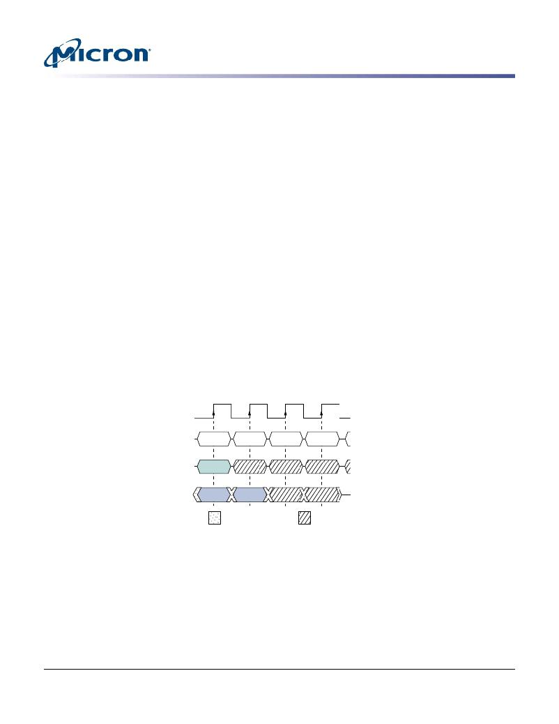
�Figure� 26:� WRITE� Burst�
�T0�
�T1�
�T2�
�T3�
�CLK�
�Command�
�WRITE�
�NOP�
�NOP�
�NOP�
�Address�
�Bank,�
�Col� n�
�DQ�
�D� IN�
�n�
�D� IN�
�n+1�
�Transitioning� data�
�Don’t� Care�
�Note:�
�1.� BL� =� 2.� DQM� is� LOW.�
�PDF:� 09005aef8459c827�
�512mb_mobile_sdram_y67m_at.pdf� –� Rev.� B� 3/11� EN�
�56�
�Micron� Technology,� Inc.� reserves� the� right� to� change� products� or� specifications� without� notice.�
�?� 2011� Micron� Technology,� Inc.� All� rights� reserved.�
�相关PDF资料 |
PDF描述 |
|---|---|
| MT48H8M16LFB4-75 IT:K TR | IC SDRAM 128MBIT 133MHZ 54VFBGA |
| MTC100-JA2-P34 | CONTACT INSERT PIN |
| MX841BE | IC CONVERTER WHITE LED 8-SOIC |
| MXHV9910BTR | IC LED DRIVER HIGH BRIGHT 8-SOIC |
| MXN12FB12F | MOTOR BRUSHED DC 12V 2922RPM |
相关代理商/技术参数 |
参数描述 |
|---|
发布紧急采购,3分钟左右您将得到回复。