参数资料
| 型号: | XC3S700A-4FT256I |
| 厂商: | Xilinx Inc |
| 文件页数: | 76/132页 |
| 文件大小: | 0K |
| 描述: | IC FPGA SPARTAN 3 256FTBGA |
| 标准包装: | 90 |
| 系列: | Spartan®-3A |
| LAB/CLB数: | 1472 |
| 逻辑元件/单元数: | 13248 |
| RAM 位总计: | 368640 |
| 输入/输出数: | 161 |
| 门数: | 700000 |
| 电源电压: | 1.14 V ~ 1.26 V |
| 安装类型: | 表面贴装 |
| 工作温度: | -40°C ~ 100°C |
| 封装/外壳: | 256-LBGA |
| 供应商设备封装: | 256-FTBGA |
第1页第2页第3页第4页第5页第6页第7页第8页第9页第10页第11页第12页第13页第14页第15页第16页第17页第18页第19页第20页第21页第22页第23页第24页第25页第26页第27页第28页第29页第30页第31页第32页第33页第34页第35页第36页第37页第38页第39页第40页第41页第42页第43页第44页第45页第46页第47页第48页第49页第50页第51页第52页第53页第54页第55页第56页第57页第58页第59页第60页第61页第62页第63页第64页第65页第66页第67页第68页第69页第70页第71页第72页第73页第74页第75页当前第76页第77页第78页第79页第80页第81页第82页第83页第84页第85页第86页第87页第88页第89页第90页第91页第92页第93页第94页第95页第96页第97页第98页第99页第100页第101页第102页第103页第104页第105页第106页第107页第108页第109页第110页第111页第112页第113页第114页第115页第116页第117页第118页第119页第120页第121页第122页第123页第124页第125页第126页第127页第128页第129页第130页第131页第132页
DC and Switching Characteristics
48
DS529-3 (v2.0) August 19, 2010
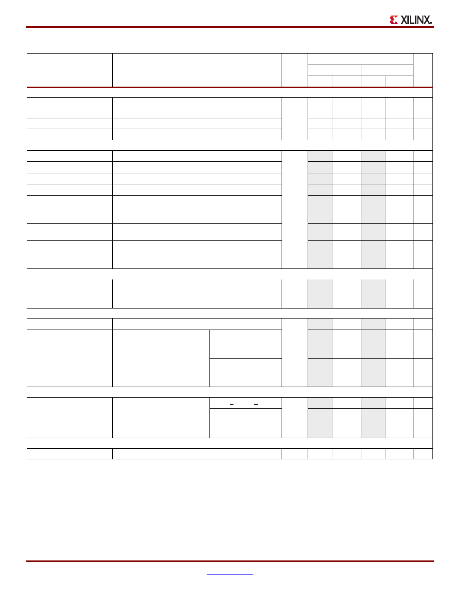
Table 37: Switching Characteristics for the DLL
Symbol
Description
Device
Speed Grade
Units
-5
-4
Min
Max
Min
Max
Output Frequency Ranges
CLKOUT_FREQ_CLK0
Frequency for the CLK0 and CLK180 outputs
All
5
280
5
250
MHz
CLKOUT_FREQ_CLK90
Frequency for the CLK90 and CLK270 outputs
5
200
5
200
MHz
CLKOUT_FREQ_2X
Frequency for the CLK2X and CLK2X180 outputs
10
334
10
334
MHz
CLKOUT_FREQ_DV
Frequency for the CLKDV output
0.3125
186
0.3125
166
MHz
Output Clock Jitter(2,3,4)
CLKOUT_PER_JITT_0
Period jitter at the CLK0 output
All
–
±100
–
±100
ps
CLKOUT_PER_JITT_90
Period jitter at the CLK90 output
–
±150
–
±150
ps
CLKOUT_PER_JITT_180
Period jitter at the CLK180 output
–
±150
–
±150
ps
CLKOUT_PER_JITT_270
Period jitter at the CLK270 output
–
±150
–
±150
ps
CLKOUT_PER_JITT_2X
Period jitter at the CLK2X and CLK2X180 outputs
–
±[0.5%
of CLKIN
period
+ 100]
–
±[0.5%
of CLKIN
period
+ 100]
ps
CLKOUT_PER_JITT_DV1
Period jitter at the CLKDV output when performing integer
division
–
±150
–
±150
ps
CLKOUT_PER_JITT_DV2
Period jitter at the CLKDV output when performing non-integer
division
–
±[0.5%
of CLKIN
period
+ 100]
–
±[0.5%
of CLKIN
period
+ 100]
ps
Duty Cycle(4)
CLKOUT_DUTY_CYCLE_DLL Duty cycle variation for the CLK0, CLK90, CLK180, CLK270,
CLK2X, CLK2X180, and CLKDV outputs, including the
BUFGMUX and clock tree duty-cycle distortion
All
–
±[1% of
CLKIN
period
+ 350]
–
±[1% of
CLKIN
period
+ 350]
ps
Phase Alignment(4)
CLKIN_CLKFB_PHASE
Phase offset between the CLKIN and CLKFB inputs
All
–
±150
–
±150
ps
CLKOUT_PHASE_DLL
Phase offset between DLL outputs
CLK0 to CLK2X
(not CLK2X180)
–
±[1% of
CLKIN
period
+ 100]
–
±[1% of
CLKIN
period
+ 100]
ps
All others
–
±[1% of
CLKIN
period
+ 150]
–
±[1% of
CLKIN
period
+ 150]
ps
Lock Time
LOCK_DLL(3)
When using the DLL alone: The
time from deassertion at the DCM’s
Reset input to the rising transition
at its LOCKED output. When the
DCM is locked, the CLKIN and
CLKFB signals are in phase
5 MHz < FCLKIN < 15 MHz
All
–
5
–
5ms
FCLKIN > 15 MHz
–
600
–
600
s
Delay Lines
DCM_DELAY_STEP(5)
Finest delay resolution, averaged over all steps
All
15
35
15
35
ps
Notes:
1.
2.
Indicates the maximum amount of output jitter that the DCM adds to the jitter on the CLKIN input.
3.
For optimal jitter tolerance and faster lock time, use the CLKIN_PERIOD attribute.
4.
Some jitter and duty-cycle specifications include 1% of input clock period or 0.01 UI. For example, the data sheet specifies a maximum jitter of
“±[1% of CLKIN period + 150]”. Assume the CLKIN frequency is 100 MHz. The equivalent CLKIN period is 10 ns and 1% of 10 ns is 0.1 ns or 100 ps.
According to the data sheet, the maximum jitter is ±[100 ps + 150 ps] = ±250ps.
5.
The typical delay step size is 23 ps.
相关PDF资料 |
PDF描述 |
|---|---|
| 93LC76AT-E/SN | IC EEPROM 8KBIT 2MHZ 8SOIC |
| XC2S100-6FG256C | IC FPGA 2.5V C-TEMP 256-FBGA |
| 24LC64T-E/OT | IC EEPROM 64KBIT 400KHZ SOT23-5 |
| 24LC16B-E/MC | IC EEPROM 16KBIT 400KHZ 8DFN |
| 93LC76A-E/SN | IC EEPROM 8KBIT 2MHZ 8SOIC |
相关代理商/技术参数 |
参数描述 |
|---|---|
| XC3S700A-4FTG256C | 功能描述:IC FPGA SPARTAN-3A 256K 256FTBGA RoHS:是 类别:集成电路 (IC) >> 嵌入式 - FPGA(现场可编程门阵列) 系列:Spartan®-3A 标准包装:40 系列:Spartan® 6 LX LAB/CLB数:3411 逻辑元件/单元数:43661 RAM 位总计:2138112 输入/输出数:358 门数:- 电源电压:1.14 V ~ 1.26 V 安装类型:表面贴装 工作温度:-40°C ~ 100°C 封装/外壳:676-BGA 供应商设备封装:676-FBGA(27x27) |
| XC3S700A-4FTG256I | 功能描述:IC FPGA SPARTAN-3A 256K 256FTBGA RoHS:是 类别:集成电路 (IC) >> 嵌入式 - FPGA(现场可编程门阵列) 系列:Spartan®-3A 标准包装:24 系列:ECP2 LAB/CLB数:1500 逻辑元件/单元数:12000 RAM 位总计:226304 输入/输出数:131 门数:- 电源电压:1.14 V ~ 1.26 V 安装类型:表面贴装 工作温度:0°C ~ 85°C 封装/外壳:208-BFQFP 供应商设备封装:208-PQFP(28x28) |
| XC3S700A-5FG400C | 功能描述:IC SPARTAN-3A FPGA 700K 400FBGA RoHS:否 类别:集成电路 (IC) >> 嵌入式 - FPGA(现场可编程门阵列) 系列:Spartan®-3A 标准包装:40 系列:Spartan® 6 LX LAB/CLB数:3411 逻辑元件/单元数:43661 RAM 位总计:2138112 输入/输出数:358 门数:- 电源电压:1.14 V ~ 1.26 V 安装类型:表面贴装 工作温度:-40°C ~ 100°C 封装/外壳:676-BGA 供应商设备封装:676-FBGA(27x27) |
| XC3S700A-5FG484C | 功能描述:IC SPARTAN-3A FPGA 700K 484FBGA RoHS:否 类别:集成电路 (IC) >> 嵌入式 - FPGA(现场可编程门阵列) 系列:Spartan®-3A 标准包装:40 系列:Spartan® 6 LX LAB/CLB数:3411 逻辑元件/单元数:43661 RAM 位总计:2138112 输入/输出数:358 门数:- 电源电压:1.14 V ~ 1.26 V 安装类型:表面贴装 工作温度:-40°C ~ 100°C 封装/外壳:676-BGA 供应商设备封装:676-FBGA(27x27) |
| XC3S700A-5FGG400C | 功能描述:IC SPARTAN-3A FPGA 700K 400FBGA RoHS:是 类别:集成电路 (IC) >> 嵌入式 - FPGA(现场可编程门阵列) 系列:Spartan®-3A 标准包装:40 系列:Spartan® 6 LX LAB/CLB数:3411 逻辑元件/单元数:43661 RAM 位总计:2138112 输入/输出数:358 门数:- 电源电压:1.14 V ~ 1.26 V 安装类型:表面贴装 工作温度:-40°C ~ 100°C 封装/外壳:676-BGA 供应商设备封装:676-FBGA(27x27) |
发布紧急采购,3分钟左右您将得到回复。