参数资料
| 型号: | ADP1046ACPZ-RL |
| 厂商: | Analog Devices Inc |
| 文件页数: | 18/92页 |
| 文件大小: | 0K |
| 描述: | IC DGTL CTRLR 32LFCSP |
| 标准包装: | 5,000 |
| 应用: | 电源 |
| 输入电压: | 0 V ~ 1.6 V |
| 电源电压: | 3 V ~ 3.6 V |
| 电流 - 电源: | 20mA |
| 工作温度: | -40°C ~ 125°C |
| 安装类型: | 表面贴装 |
| 封装/外壳: | 32-WFQFN 裸露焊盘,CSP |
| 供应商设备封装: | 32-LFCSP-WQ(5x5) |
| 包装: | 带卷 (TR) |
第1页第2页第3页第4页第5页第6页第7页第8页第9页第10页第11页第12页第13页第14页第15页第16页第17页当前第18页第19页第20页第21页第22页第23页第24页第25页第26页第27页第28页第29页第30页第31页第32页第33页第34页第35页第36页第37页第38页第39页第40页第41页第42页第43页第44页第45页第46页第47页第48页第49页第50页第51页第52页第53页第54页第55页第56页第57页第58页第59页第60页第61页第62页第63页第64页第65页第66页第67页第68页第69页第70页第71页第72页第73页第74页第75页第76页第77页第78页第79页第80页第81页第82页第83页第84页第85页第86页第87页第88页第89页第90页第91页第92页
�� �
�
�2� f� SW� +� s�
�2� f� SW� ?� s�
�ADP1046�
�To� transfer� the� z-domain� value� to� the� s-domain,� plug� the� follow-�
�ing� bilinear� transformation� equation� into� the� H(z)� equation:�
�z(s)� =�
�The� digital� filter� introduces� an� extra� phase� delay� element� into�
�the� control� loop.� The� digital� filter� circuit� sends� the� duty� cycle�
�information� to� the� PWM� circuit� at� the� beginning� of� each� switch-�
�ing� cycle� (unlike� an� analog� controller,� which� makes� decisions� on�
�the� duty� cycle� information� continuously).� Therefore,� the� extra�
�phase� delay� for� phase� margin,� Φ,� introduced� by� the� filter� block� is�
�Φ� =� 360� ×� (� f� C� /� f� SW� )�
�where:�
�f� C� is� the� crossover� frequency.�
�Data� Sheet�
�PWM� AND� SYNC� RECT� OUTPUTS� (OUTA,� OUTB,�
�OUTC,� OUTD,� OUTAUX,� SR1,� SR2)�
�The� PWM� and� SR� outputs� are� used� for� control� of� the� primary�
�side� drivers� and� the� synchronous� rectifier� drivers.� These� outputs�
�can� be� used� for� several� control� topologies� such� as� full-bridge,�
�phase-shifted� ZVS� configurations� and� interleaved,� two� switch�
�forward� converter� configurations.� Delays� between� rising� and�
�falling� edges� can� be� individually� programmed.� Special� care�
�must� be� taken� to� avoid� shootthrough� and� cross-conduction.�
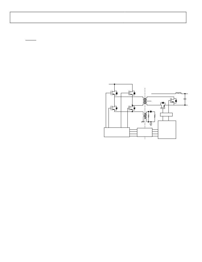
�It� is� recommended� that� the� Analog� Devices� software� GUI� be�
�used� to� program� these� outputs.� Figure� 20� shows� an� example�
�configuration� to� drive� a� full-bridge,� phase-shifted� topology�
�with� synchronous� rectification.�
�V� IN�
�f� SW� is� the� switching� frequency.�
�At� one-tenth� the� switching� frequency,� the� phase� delay� is� 36°.�
�The� GUI� incorporates� this� phase� delay� into� its� calculations.�
�OUTA�
�OUTC�
�Note� that� the� GUI� does� not� account� for� other� delays� such� as�
�SR1�
�SR2�
�gate� driver� and� propagation� delays.�
�Two� sets� of� registers� allow� for� two� distinct� filter� responses.�
�The� main� filter,� called� the� normal� mode� filter,� is� controlled� by�
�programming� Register� 0x60� to� Register� 0x63.� The� light� load�
�OUTB�
�OUTD�
�DRIVER�
�mode� filter� is� controlled� by� programming� Register� 0x64� to�
�Register� 0x67.� The� ADP1046� uses� the� light� load� mode� filter�
�SR1�
�SR2�
�only� when� the� output� current� measured� on� CS2±� is� below� the�
�load� current� threshold� (programmed� using� Register� 0x3B[2:0]).�
�DRIVER�
�ISOLATOR�
�OUTA�
�OUTB�
�OUTC�
�OUTD�
�The� Analog� Devices� software� GUI� allows� the� user� to� program� the�
�light� load� mode� filter� in� the� same� manner� as� the� normal� mode�
�filter.� It� is� recommended� that� the� GUI� be� used� for� this� purpose.�
�In� addition,� during� the� soft� start� process,� a� soft� start� filter� can�
�be� used� in� combination� with� the� normal� mode� filter� and� the�
�light� load� mode� filter.� The� soft� start� filter� is� programmed� using�
�Register� 0x71� to� Register� 0x74.� For� more� information,� see� the�
��Filter� Transitions�
�To� avoid� output� voltage� glitches� and� provide� a� seamless�
�transition� from� one� filter� to� another,� the� ADP1046� supports�
�programmable� filter� transitions.� This� feature� allows� a� gradual�
�transition� from� one� filter� to� another.� Filter� transitions� are�
�programmed� using� Register� 0x7A[2:0].�
�Figure� 20.� PWM� Pin� Assignment� for� Full-Bridge,� Phase-Shifted� Topology�
�with� Synchronous� Rectification�
�The� PWM� and� SR� outputs� are� all� synchronized� with� each�
�other.� Therefore,� when� reprogramming� more� than� one� of� these�
�outputs,� it� is� important� to� first� update� all� the� registers� and� then�
�latch� the� information� into� the� ADP1046� at� the� same� time.� During�
�reprogramming,� the� outputs� are� temporarily� disabled.� A� special�
�instruction� is� sent� to� the� ADP1046� to� ensure� that� new� timing�
�information� is� programmed� simultaneously.� This� is� done� by�
�setting� Bit� 1� in� Register� 0x7F.� It� is� recommended� that� PWM�
�outputs� be� disabled� when� not� in� use.�
�OUTAUX� is� an� additional� PWM� output� pin.� OUTAUX� allows�
�an� extra� PWM� signal� to� be� generated� at� a� different� frequency�
�from� the� other� six� PWM� outputs.� This� signal� can� be� used� to�
�drive� an� extra� power� converter� stage,� such� as� a� buck� controller�
�located� in� front� of� a� full-bridge� converter.� OUTAUX� can� also�
�be� used� as� a� clock� reference� signal.�
�For� more� information� about� the� various� programmable� switching�
���Rev.� B� |� Page� 18� of� 92�
�相关PDF资料 |
PDF描述 |
|---|---|
| ADP1111ANZ-12 | IC REG BUCK BST INV 12V .2A 8DIP |
| ADP121-ACBZ12R7 | IC REG LDO 1.2V .15A 4WLCSP |
| ADP122AUJZ-2.9-R7 | IC REG LDO 2.9V .3A 5TSOT |
| ADP124ARHZ-2.85-R7 | IC REG LDO 2.85V .5A 8MSOP |
| ADP130AUJZ-2.5-R7 | IC REG LDO 2.5V .35A TSOT-23-5 |
相关代理商/技术参数 |
参数描述 |
|---|---|
| ADP1046ADC1-EVALZ | 功能描述:电源管理IC开发工具 RoHS:否 制造商:Maxim Integrated 产品:Evaluation Kits 类型:Battery Management 工具用于评估:MAX17710GB 输入电压: 输出电压:1.8 V |
| ADP1046AWACPZ-R7 | 功能描述:Power Supply Controller Power Supplies 32-LFCSP-WQ (5x5) 制造商:analog devices inc. 系列:- 包装:剪切带(CT) 零件状态:有效 应用:电源 电压 - 输入:0 V ~ 1.6 V 电压 - 电源:3 V ~ 3.6 V 电流 - 电源:20mA 工作温度:-40°C ~ 125°C 安装类型:表面贴装 封装/外壳:32-WFQFN 裸露焊盘,CSP 供应商器件封装:32-LFCSP-WQ(5x5) 标准包装:1 |
| ADP1046DC1-EVALZ | 功能描述:BOARD EVAL DAUGHTERCARD ADP1046 RoHS:是 类别:编程器,开发系统 >> 评估演示板和套件 系列:- 标准包装:1 系列:PSoC® 主要目的:电源管理,热管理 嵌入式:- 已用 IC / 零件:- 主要属性:- 次要属性:- 已供物品:板,CD,电源 |
| ADP1047 | 制造商:AD 制造商全称:Analog Devices 功能描述:Digital Power Factor Correction Controller |
| ADP1047-300-EVALZ | 制造商:Analog Devices 功能描述:ANAADP1047-300-EVALZ 300W EVALUATION BOA 制造商:Analog Devices 功能描述:EVAL DIGITAL PFC CONTROLLER 300W 制造商:Analog Devices 功能描述:ADP1047, PFC CNTLR, 300W, EVAL KIT |
发布紧急采购,3分钟左右您将得到回复。