参数资料
| 型号: | ADP1046ACPZ-RL |
| 厂商: | Analog Devices Inc |
| 文件页数: | 42/92页 |
| 文件大小: | 0K |
| 描述: | IC DGTL CTRLR 32LFCSP |
| 标准包装: | 5,000 |
| 应用: | 电源 |
| 输入电压: | 0 V ~ 1.6 V |
| 电源电压: | 3 V ~ 3.6 V |
| 电流 - 电源: | 20mA |
| 工作温度: | -40°C ~ 125°C |
| 安装类型: | 表面贴装 |
| 封装/外壳: | 32-WFQFN 裸露焊盘,CSP |
| 供应商设备封装: | 32-LFCSP-WQ(5x5) |
| 包装: | 带卷 (TR) |
第1页第2页第3页第4页第5页第6页第7页第8页第9页第10页第11页第12页第13页第14页第15页第16页第17页第18页第19页第20页第21页第22页第23页第24页第25页第26页第27页第28页第29页第30页第31页第32页第33页第34页第35页第36页第37页第38页第39页第40页第41页当前第42页第43页第44页第45页第46页第47页第48页第49页第50页第51页第52页第53页第54页第55页第56页第57页第58页第59页第60页第61页第62页第63页第64页第65页第66页第67页第68页第69页第70页第71页第72页第73页第74页第75页第76页第77页第78页第79页第80页第81页第82页第83页第84页第85页第86页第87页第88页第89页第90页第91页第92页
�� �
�
�ADP1046�
�WRITE� OPERATION� (BYTE� WRITE� AND� BLOCK�
�WRITE)�
�Write� to� Main� Block,� Page� 0� and� Page� 1�
�Page� 0� and� Page� 1� of� the� main� block� are� reserved� for� storing� the�
�default� settings� and� user� settings,� respectively.� The� user� cannot�
�perform� a� direct� write� operation� to� Page� 0� or� Page� 1� using� the�
�EEPROM_DATA_00� and� EEPROM_DATA_01� commands.� A�
�user� write� to� Page� 0� or� Page� 1� returns� a� no� acknowledge.� To�
�program� the� register� contents� of� Page� 1� of� the� main� block,� it� is�
�recommended� that� the� STORE_USER_ALL� command� be� used�
��section.�
�Write� to� Main� Block,� Page� 2� and� Page� 3�
�Page� 2� and� Page� 3� of� the� main� block� are� reserved� for� internal�
�use� and� their� contents� should� not� be� written� to.� Only� Page� 4�
�to� Page� 15� should� be� used� to� store� data.�
�Write� to� Main� Block,� Page� 4� to� Page� 15�
�Before� performing� a� write� to� Page� 4� through� Page� 15� of� the�
�main� block,� the� user� must� first� unlock� the� EEPROM� (see� the�
��Data� in� Page� 4� to� Page� 15� of� the� EEPROM� main� block� can� be�
�programmed� (written� to)� one� byte� at� a� time� or� in� multiple� bytes� in�
�series� using� the� EEPROM_DATA_xx� commands� (Register� 0x8B�
�to� Register� 0x9A).� Before� executing� this� command,� the� user� can�
�program� the� offset� from� the� page� boundary� where� the� first� byte�
�is� written� using� the� EEPROM_ADDR_OFFSET� command�
�(Register� 0x85).�
�If� the� targeted� page� has� not� yet� been� erased,� the� user� can� erase�
�the� page� as� described� in� the� Page� Erase� Operation� section.�
�In� the� following� example,� four� bytes� are� written� to� Page� 9,�
�starting� from� the� 256� th� byte� of� that� page.�
�1.� Set� address� offset� =� 256.�
�Data� Sheet�
�EEPROM� PASSWORD�
�On� power-up,� the� EEPROM� is� locked� and� protected� from�
�accidental� writes� or� erases.� Only� reads� from� Page� 2� to� Page� 15�
�of� the� main� block� are� allowed� when� the� EEPROM� is� locked.�
�Before� any� data� can� be� written� (programmed)� to� the� EEPROM,�
�the� EEPROM� must� be� unlocked� for� write� access.� After� it� is�
�unlocked,� the� EEPROM� is� opened� for� reading,� writing,� and�
�erasing.�
�Unlock� the� EEPROM�
�To� unlock� the� EEPROM,� perform� two� consecutive� writes�
�with� the� correct� password� (default� =� 0xFF)� using� the� EEPROM_�
�PASSWORD� command� (Register� 0x88).� The� EEPROM� unlocked�
�flag� (Bit� 0� of� Register� 0x03)� is� set� to� indicate� that� the� EEPROM�
�is� unlocked� for� write� access.�
�Lock� the� EEPROM�
�To� lock� the� EEPROM,� write� any� byte� other� than� the� correct� pass-�
�word� using� the� EEPROM_PASSWORD� command� (Register� 0x88).�
�The� EEPROM� unlocked� flag� (Bit� 0� of� Register� 0x03)� is� cleared�
�to� indicate� that� the� EEPROM� is� locked� from� write� access.�
�Change� the� EEPROM� Password�
�To� change� the� EEPROM� password,� first� write� the� correct� password�
�using� the� EEPROM_PASSWORD� command� (Register� 0x88).�
�Immediately� write� the� new� password� using� the� same� command.�
�The� password� is� now� changed� to� the� new� password.�
�DOWNLOADING� EEPROM� SETTINGS� TO� INTERNAL�
�REGISTERS�
�Download� User� Settings� to� Registers�
�The� user� settings� are� stored� in� Page� 1� of� the� EEPROM� main�
�block.� These� settings� are� downloaded� from� the� EEPROM� into�
�the� registers� under� the� following� conditions:�
�?� On� power-up.� The� user� settings� are� automatically� down-�
�loaded� into� the� internal� registers,� powering� the� part� up� in�
�S�
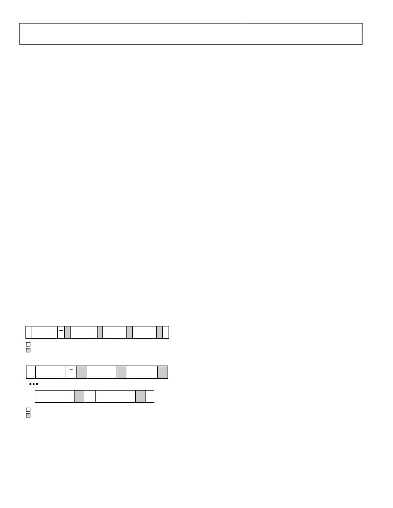
�7-BIT�
�SLAVE�
�ADDRESS�
�W� A�
�0x85�
�A�
�0x00�
�A�
�0x01�
�A� P�
�?�
�a� state� previously� saved� by� the� user.�
�On� execution� of� the� RESTORE_USER_ALL� command�
�2.�
�=� MASTER-TO-SLAVE�
�=� SLAVE-TO-MASTER�
�Write� four� bytes� to� Page� 9.�
�(Register� 0x83).� This� command� allows� the� user� to� force� a�
�download� of� the� user� settings� from� Page� 1� of� the� EEPROM�
�main� block� into� the� internal� registers.�
�S�
�7-BIT�
�SLAVE�
�ADDRESS�
�W�
�A�
�0x94�
�A�
�BYTE�
�COUNT� =� 4�
�A�
�Download� Factory� Default� Settings� to� Registers�
�The� factory� default� settings� are� stored� in� Page� 0� of� the� EEPROM�
�DATA� BYTE� 1�
�A�
�...�
�DATA� BYTE� 4�
�A�
�P�
�main� block.� The� factory� default� settings� can� be� downloaded� from�
�the� EEPROM� into� the� internal� registers� using� the� RESTORE_�
�=� MASTER-TO-SLAVE�
�=� SLAVE-TO-MASTER�
�Note� that� the� block� write� command� can� write� a� maximum�
�of� 256� bytes� for� any� single� transaction� (set� the� byte� count� =� 0).�
�DEFAULT_ALL� command� (Register� 0x81).�
�When� this� command� is� executed,� the� EEPROM� password� is� also�
�reset� to� the� factory� default� setting� of� 0xFF.�
�Rev.� B� |� Page� 42� of� 92�
�相关PDF资料 |
PDF描述 |
|---|---|
| ADP1111ANZ-12 | IC REG BUCK BST INV 12V .2A 8DIP |
| ADP121-ACBZ12R7 | IC REG LDO 1.2V .15A 4WLCSP |
| ADP122AUJZ-2.9-R7 | IC REG LDO 2.9V .3A 5TSOT |
| ADP124ARHZ-2.85-R7 | IC REG LDO 2.85V .5A 8MSOP |
| ADP130AUJZ-2.5-R7 | IC REG LDO 2.5V .35A TSOT-23-5 |
相关代理商/技术参数 |
参数描述 |
|---|---|
| ADP1046ADC1-EVALZ | 功能描述:电源管理IC开发工具 RoHS:否 制造商:Maxim Integrated 产品:Evaluation Kits 类型:Battery Management 工具用于评估:MAX17710GB 输入电压: 输出电压:1.8 V |
| ADP1046AWACPZ-R7 | 功能描述:Power Supply Controller Power Supplies 32-LFCSP-WQ (5x5) 制造商:analog devices inc. 系列:- 包装:剪切带(CT) 零件状态:有效 应用:电源 电压 - 输入:0 V ~ 1.6 V 电压 - 电源:3 V ~ 3.6 V 电流 - 电源:20mA 工作温度:-40°C ~ 125°C 安装类型:表面贴装 封装/外壳:32-WFQFN 裸露焊盘,CSP 供应商器件封装:32-LFCSP-WQ(5x5) 标准包装:1 |
| ADP1046DC1-EVALZ | 功能描述:BOARD EVAL DAUGHTERCARD ADP1046 RoHS:是 类别:编程器,开发系统 >> 评估演示板和套件 系列:- 标准包装:1 系列:PSoC® 主要目的:电源管理,热管理 嵌入式:- 已用 IC / 零件:- 主要属性:- 次要属性:- 已供物品:板,CD,电源 |
| ADP1047 | 制造商:AD 制造商全称:Analog Devices 功能描述:Digital Power Factor Correction Controller |
| ADP1047-300-EVALZ | 制造商:Analog Devices 功能描述:ANAADP1047-300-EVALZ 300W EVALUATION BOA 制造商:Analog Devices 功能描述:EVAL DIGITAL PFC CONTROLLER 300W 制造商:Analog Devices 功能描述:ADP1047, PFC CNTLR, 300W, EVAL KIT |
发布紧急采购,3分钟左右您将得到回复。