参数资料
| 型号: | ADP1046ACPZ-RL |
| 厂商: | Analog Devices Inc |
| 文件页数: | 37/92页 |
| 文件大小: | 0K |
| 描述: | IC DGTL CTRLR 32LFCSP |
| 标准包装: | 5,000 |
| 应用: | 电源 |
| 输入电压: | 0 V ~ 1.6 V |
| 电源电压: | 3 V ~ 3.6 V |
| 电流 - 电源: | 20mA |
| 工作温度: | -40°C ~ 125°C |
| 安装类型: | 表面贴装 |
| 封装/外壳: | 32-WFQFN 裸露焊盘,CSP |
| 供应商设备封装: | 32-LFCSP-WQ(5x5) |
| 包装: | 带卷 (TR) |
第1页第2页第3页第4页第5页第6页第7页第8页第9页第10页第11页第12页第13页第14页第15页第16页第17页第18页第19页第20页第21页第22页第23页第24页第25页第26页第27页第28页第29页第30页第31页第32页第33页第34页第35页第36页当前第37页第38页第39页第40页第41页第42页第43页第44页第45页第46页第47页第48页第49页第50页第51页第52页第53页第54页第55页第56页第57页第58页第59页第60页第61页第62页第63页第64页第65页第66页第67页第68页第69页第70页第71页第72页第73页第74页第75页第76页第77页第78页第79页第80页第81页第82页第83页第84页第85页第86页第87页第88页第89页第90页第91页第92页
�� ��
��
��S�
�W�
�A�
�A�
�...�
�P�
�ADDRESS�
�Data� Sheet�
�I� 2� C� INTERFACE� COMMUNICATION�
�The� ADP1046� I� 2� C� slave� is� a� 2-wire� interface� that� can� be� used�
�to� communicate� with� other� I� 2� C-compliant� master� devices� and�
�is� compatible� in� a� multimaster,� multislave� bus� configuration.�
�FEATURES�
�The� function� of� the� I� 2� C� slave� is� to� decode� the� command� sent� from�
�the� master� device� and� respond� as� requested.� Communication� is�
�established� using� a� 2-wire� interface� with� a� clock� line� (SCL)� and�
�data� line� (SDA).� The� I� 2� C� slave� is� designed� to� externally� move�
�chunks� of� 8-bit� data� (bytes)� while� maintaining� compliance� with�
�the� I� 2� C� protocol,� based� on� the� Philips� I� 2� C� Bus� Specification� ,�
�Version� 2.1,� dated� January� 2000.� The� I� 2� C� protocol� incorporates�
�the� following� features:�
�?� Slave� operation� on� multiple� device� systems�
�?� 7-bit� addressing�
�?� 100� kB/sec� and� 400� kB/sec� data� rates�
�?� General� call� address� support�
�?� Support� for� clock� low� extension� (clock� stretching)�
�?� Separate� multiple� byte� receive� and� transmit� FIFO�
�?� Extensive� communication� fault� monitoring�
�OVERVIEW�
�The� I� 2� C� slave� module� is� a� 2-wire� interface� that� can� be� used� to�
�communicate� with� other� I� 2� C-compliant� master� devices.� Its� trans-�
�fer� protocol� is� based� on� the� Philips� I� 2� C� transfer� mechanism.� The�
�ADP1046� is� always� configured� as� a� slave� device� in� the� overall�
�system.� The� ADP1046� communicates� with� the� master� device�
�using� one� data� pin� (SDA)� and� one� clock� pin� (SCL).� Because� the�
�ADP1046� is� a� slave� device,� it� cannot� generate� the� clock� signal.�
�However,� it� is� capable� of� stretching� the� SCL� line� to� put� the�
�master� device� in� a� wait� state� when� it� is� not� ready� to� respond�
�ADP1046�
�I� 2� C� ADDRESS�
�The� I� 2� C� address� of� the� ADP1046� is� set� by� connecting� an�
�external� resistor� from� the� ADD� pin� to� AGND.� Table� 6� lists� the�
�recommended� resistor� values� and� the� associated� I� 2� C� addresses.�
�Seven� different� addresses� can� be� used.�
�The� recommended� resistor� values� in� Table� 6� must� be� 1%�
�tolerance� resistors.�
�Table� 6.� Recommended� Resistor� Values� for� I� 2� C� Addresses�
�I� 2� C� Address� Resistor� Value� (kΩ)�
�0x50� 10� (or� connect� the� ADD� pin� directly� to� AGND)�
�0x51� 28.7�
�0x52� 48.7�
�0x53� 68.1�
�0x54� 88.7�
�0x55� 109�
�0x57� 200� (or� connect� the� ADD� pin� directly� to� VDD)�
�DATA� TRANSFER�
�Format� Overview�
�The� I� 2� C� slave� follows� the� transfer� protocol� of� the� Philips� I� 2� C� Bus�
�Specification� .� Data� transfers� are� byte-wide,� lower� byte� first.� Each�
�byte� is� transmitted� serially,� most� significant� bit� (MSB)� first.� A�
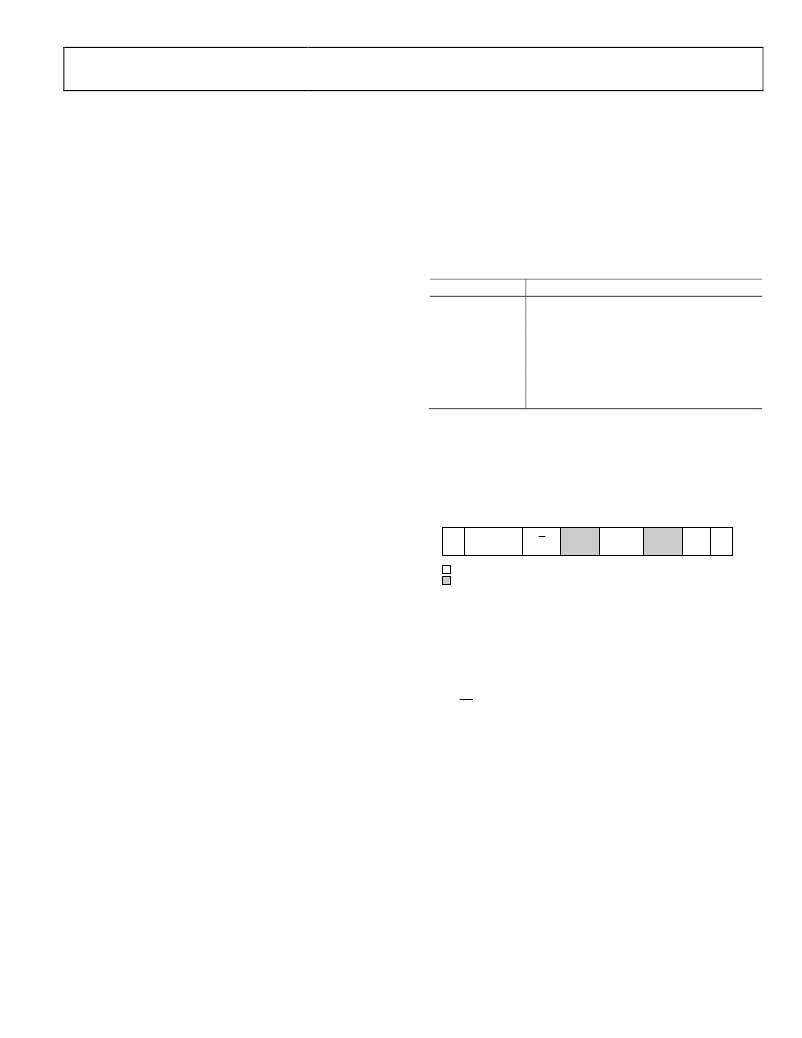
��7-BIT� SLAVE� 8-BIT�
�DATA�
�=� MASTER-TO-SLAVE�
�=� SLAVE-TO-MASTER�
�Figure� 45.� Basic� Data� Transfer�
��to� the� master’s� request.�
�?�
�S� =� start� condition�
�Communication� is� initiated� when� the� master� device� sends� a�
�command� to� the� I� 2� C� slave� device.� Commands� can� be� read� or�
�write� commands,� in� which� case� data� is� transferred� between� the�
�devices� in� a� byte-wide� format.� Commands� can� also� be� send�
�commands,� in� which� case� the� command� is� executed� by� the� slave�
�device� upon� receiving� the� stop� bit.� The� stop� bit� is� the� last� bit� in�
�a� complete� data� transfer,� as� defined� in� the� I� 2� C� communication�
�protocol.� During� communication,� the� master� and� slave� devices�
�send� acknowledge� (A)� or� no� acknowledge� (NA)� bits� as� a� method�
�of� handshaking� between� devices.� Refer� to� the� Philips� I� 2� C� Bus�
�?� Sr� =� repeated� start� condition�
�?� P� =� stop� condition�
�?� R� =� read� bit�
�?� W� =� write� bit�
�?� A� =� acknowledge� bit� (0)�
�?� NA� =� no� acknowledge� bit� (1)�
�Refer� to� the� I� 2� C� specification� for� an� in-depth� discussion� of� the�
�transfer� protocols.�
�Specification� ,� Version� 2.1,� dated� January� 2000,� for� a� more� detailed�
�description� of� the� communication� protocol.�
�Rev.� B� |� Page� 37� of� 92�
�相关PDF资料 |
PDF描述 |
|---|---|
| ADP1111ANZ-12 | IC REG BUCK BST INV 12V .2A 8DIP |
| ADP121-ACBZ12R7 | IC REG LDO 1.2V .15A 4WLCSP |
| ADP122AUJZ-2.9-R7 | IC REG LDO 2.9V .3A 5TSOT |
| ADP124ARHZ-2.85-R7 | IC REG LDO 2.85V .5A 8MSOP |
| ADP130AUJZ-2.5-R7 | IC REG LDO 2.5V .35A TSOT-23-5 |
相关代理商/技术参数 |
参数描述 |
|---|---|
| ADP1046ADC1-EVALZ | 功能描述:电源管理IC开发工具 RoHS:否 制造商:Maxim Integrated 产品:Evaluation Kits 类型:Battery Management 工具用于评估:MAX17710GB 输入电压: 输出电压:1.8 V |
| ADP1046AWACPZ-R7 | 功能描述:Power Supply Controller Power Supplies 32-LFCSP-WQ (5x5) 制造商:analog devices inc. 系列:- 包装:剪切带(CT) 零件状态:有效 应用:电源 电压 - 输入:0 V ~ 1.6 V 电压 - 电源:3 V ~ 3.6 V 电流 - 电源:20mA 工作温度:-40°C ~ 125°C 安装类型:表面贴装 封装/外壳:32-WFQFN 裸露焊盘,CSP 供应商器件封装:32-LFCSP-WQ(5x5) 标准包装:1 |
| ADP1046DC1-EVALZ | 功能描述:BOARD EVAL DAUGHTERCARD ADP1046 RoHS:是 类别:编程器,开发系统 >> 评估演示板和套件 系列:- 标准包装:1 系列:PSoC® 主要目的:电源管理,热管理 嵌入式:- 已用 IC / 零件:- 主要属性:- 次要属性:- 已供物品:板,CD,电源 |
| ADP1047 | 制造商:AD 制造商全称:Analog Devices 功能描述:Digital Power Factor Correction Controller |
| ADP1047-300-EVALZ | 制造商:Analog Devices 功能描述:ANAADP1047-300-EVALZ 300W EVALUATION BOA 制造商:Analog Devices 功能描述:EVAL DIGITAL PFC CONTROLLER 300W 制造商:Analog Devices 功能描述:ADP1047, PFC CNTLR, 300W, EVAL KIT |
发布紧急采购,3分钟左右您将得到回复。