参数资料
| 型号: | ADP1046ACPZ-RL |
| 厂商: | Analog Devices Inc |
| 文件页数: | 19/92页 |
| 文件大小: | 0K |
| 描述: | IC DGTL CTRLR 32LFCSP |
| 标准包装: | 5,000 |
| 应用: | 电源 |
| 输入电压: | 0 V ~ 1.6 V |
| 电源电压: | 3 V ~ 3.6 V |
| 电流 - 电源: | 20mA |
| 工作温度: | -40°C ~ 125°C |
| 安装类型: | 表面贴装 |
| 封装/外壳: | 32-WFQFN 裸露焊盘,CSP |
| 供应商设备封装: | 32-LFCSP-WQ(5x5) |
| 包装: | 带卷 (TR) |
第1页第2页第3页第4页第5页第6页第7页第8页第9页第10页第11页第12页第13页第14页第15页第16页第17页第18页当前第19页第20页第21页第22页第23页第24页第25页第26页第27页第28页第29页第30页第31页第32页第33页第34页第35页第36页第37页第38页第39页第40页第41页第42页第43页第44页第45页第46页第47页第48页第49页第50页第51页第52页第53页第54页第55页第56页第57页第58页第59页第60页第61页第62页第63页第64页第65页第66页第67页第68页第69页第70页第71页第72页第73页第74页第75页第76页第77页第78页第79页第80页第81页第82页第83页第84页第85页第86页第87页第88页第89页第90页第91页第92页
�� �
�
�Data� Sheet�
�SYNCHRONOUS� RECTIFICATION�
�SR1� and� SR2� are� recommended� for� use� as� the� PWM� control�
�signals� when� using� synchronous� rectification.� These� PWM�
�signals� can� be� configured� much� like� the� other� PWM� outputs.�
�An� optional� soft� start� can� be� applied� to� the� synchronous�
�rectifier� PWM� outputs.� The� SR� soft� start� can� be� programmed�
�using� Register� 0x54[1:0].�
�?� When� SR� soft� start� is� disabled� (Register� 0x54[0]� =� 0),�
�the� SR� signals� are� turned� on� to� their� full� PWM� duty� cycle�
�values� immediately.�
�?� When� SR� soft� start� is� enabled� (Register� 0x54[0]� =� 1),� the�
�SR� signals� ramp� up� from� zero� duty� cycle� to� the� desired�
�duty� cycle� in� steps� of� 40� ns� per� switching� cycle.�
�The� advantage� of� ramping� the� SR� signals� is� to� minimize� the�
�output� voltage� step� that� occurs� when� the� SR� FETs� are� turned�
�on� without� a� soft� start.� The� advantage� of� turning� the� SR� signals�
�completely� on� immediately� is� that� they� can� help� to� minimize�
�the� voltage� transient� caused� by� a� load� step.�
�Using� Register� 0x54[1],� the� SR� soft� start� can� be� programmed� to�
�occur� only� once� (the� first� time� that� the� SR� signals� are� enabled)�
�or� every� time� that� the� SR� signals� are� enabled,� for� example,� when�
�the� system� enters� or� exits� light� load� mode.�
�When� programming� the� ADP1046� to� use� SR� soft� start,� ensure�
�ADP1046�
�To� prevent� the� system� from� oscillating� between� light� load�
�and� normal� modes� due� to� the� thresholds� being� programmed�
�too� close� to� each� other,� a� programmable� debounce� is� provided�
�in� Register� 0x7D[5:4].� This� debounce� prevents� the� part� from�
�changing� state� within� the� programmed� interval.�
�The� speed� of� the� SR� enable� is� programmable� from� 37.5� μs� to� 300� μs�
�in� four� discrete� steps� using� Register� 0x7D[3:2].� This� ensures� that,�
�in� case� of� a� load� step,� the� SR� signals� (and� any� other� PWM� outputs�
�that� are� temporarily� disabled)� can� be� turned� on� quickly� enough� to�
�prevent� damage� to� the� FETs� that� they� are� controlling.�
�The� light� load� mode� digital� filter� is� also� used� during� light�
�load� mode.�
�MODULATION� LIMIT�
�The� modulation� limit� register� (Register� 0x2E)� can� be�
�programmed� to� apply� a� maximum� duty� cycle� modulation� limit�
�to� any� PWM� signal,� thus� limiting� the� modulation� range� of� any�
�PWM� output.� When� modulation� is� enabled,� the� maximum�
�modulation� limit� is� applied� to� all� PWM� outputs� collectively.� As�
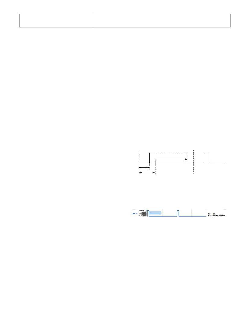
�shown� in� Figure� 21,� this� limit� is� the� maximum� time� variation�
�for� the� modulated� edges� from� the� default� timing,� following� the�
�configured� modulation� direction.� There� is� no� minimum� duty�
�cycle� limit� setting.� Therefore,� the� user� must� set� the� rising� edges�
�and� falling� edges� based� on� the� case� with� the� least� modulation.�
�correct� operation� of� this� function� by� setting� the� falling� edge� of�
�SR1� (t� 10� )� to� a� lower� value� than� the� rising� edge� of� SR1� (t� 9� )� and� by�
�OUTx�
�t� MODULATION_LIMIT�
�setting� the� falling� edge� of� SR2� (t� 12� )� to� a� lower� value� than� the� rising�
�edge� of� SR2� (t� 11� ).� SR� soft� start� can� also� be� disabled� by� setting�
�Register� 0x0F[7]� =� 1.�
�SR� (SYNCHRONOUS� RECTIFIER)� DELAY�
�The� ADP1046� is� well� suited� for� dc-to-dc� converters� in� isolated�
�topologies.� Every� time� a� PWM� signal� crosses� the� isolation� barrier�
�an� additional� propagation� delay� is� added� due� to� the� isolating�
�components.� The� ADP1046� allows� programming� of� an� adjustable�
�delay� (0� ns� to� 315� ns� in� steps� of� 5� ns)� using� Register� 0x79[5:0].� This�
�delay� moves� both� SR1� and� SR2� later� in� time� to� compensate� for� the�
�added� delay� due� to� the� isolating� components� (see� Figure� 56).� In�
�this� way,� the� edges� of� all� PWM� outputs� can� be� aligned,� and� the�
�t� RX�
�t� FX�
�Figure� 21.� Modulation� Limit� Settings�
�Each� LSB� in� Register� 0x2E� corresponds� to� a� different� time� step�
�size,� depending� on� the� switching� frequency� (see� Table� 46).� The�
�modulated� edges� cannot� extend� beyond� one� switching� cycle.�
�The� GUI� provided� with� the� ADP1046� is� recommended� for�
��Figure� 22.� Setting� Modulation� Limits� (Modulation� Range� Shown� by� Arrows)�
�SR� delay� can� be� applied� separately� as� a� constant� dead� time.�
�LIGHT� LOAD� MODE�
�The� ADP1046� can� be� configured� to� disable� PWM� outputs� under�
�light� load� conditions� based� on� the� value� of� CS2.� Register� 0x3B�
�and� Register� 0x7D� are� used� to� program� the� light� load� mode�
�thresholds� for� turn-off� and� turn-on� of� SR1,� SR2,� and� other�
�PWM� outputs.� Below� the� light� load� threshold� programmed� in�
�Register� 0x3B,� the� SR� outputs� are� disabled;� the� user� can� also�
�program� any� of� the� other� PWM� outputs� to� shut� down� below�
�this� threshold.� Light� load� mode� allows� the� ADP1046� to� be� used�
�with� interleaved� topologies� that� incorporate� automatic� phase�
�shedding� at� light� load.�
�Rev.� B� |� Page� 19� of� 92�
�相关PDF资料 |
PDF描述 |
|---|---|
| ADP1111ANZ-12 | IC REG BUCK BST INV 12V .2A 8DIP |
| ADP121-ACBZ12R7 | IC REG LDO 1.2V .15A 4WLCSP |
| ADP122AUJZ-2.9-R7 | IC REG LDO 2.9V .3A 5TSOT |
| ADP124ARHZ-2.85-R7 | IC REG LDO 2.85V .5A 8MSOP |
| ADP130AUJZ-2.5-R7 | IC REG LDO 2.5V .35A TSOT-23-5 |
相关代理商/技术参数 |
参数描述 |
|---|---|
| ADP1046ADC1-EVALZ | 功能描述:电源管理IC开发工具 RoHS:否 制造商:Maxim Integrated 产品:Evaluation Kits 类型:Battery Management 工具用于评估:MAX17710GB 输入电压: 输出电压:1.8 V |
| ADP1046AWACPZ-R7 | 功能描述:Power Supply Controller Power Supplies 32-LFCSP-WQ (5x5) 制造商:analog devices inc. 系列:- 包装:剪切带(CT) 零件状态:有效 应用:电源 电压 - 输入:0 V ~ 1.6 V 电压 - 电源:3 V ~ 3.6 V 电流 - 电源:20mA 工作温度:-40°C ~ 125°C 安装类型:表面贴装 封装/外壳:32-WFQFN 裸露焊盘,CSP 供应商器件封装:32-LFCSP-WQ(5x5) 标准包装:1 |
| ADP1046DC1-EVALZ | 功能描述:BOARD EVAL DAUGHTERCARD ADP1046 RoHS:是 类别:编程器,开发系统 >> 评估演示板和套件 系列:- 标准包装:1 系列:PSoC® 主要目的:电源管理,热管理 嵌入式:- 已用 IC / 零件:- 主要属性:- 次要属性:- 已供物品:板,CD,电源 |
| ADP1047 | 制造商:AD 制造商全称:Analog Devices 功能描述:Digital Power Factor Correction Controller |
| ADP1047-300-EVALZ | 制造商:Analog Devices 功能描述:ANAADP1047-300-EVALZ 300W EVALUATION BOA 制造商:Analog Devices 功能描述:EVAL DIGITAL PFC CONTROLLER 300W 制造商:Analog Devices 功能描述:ADP1047, PFC CNTLR, 300W, EVAL KIT |
发布紧急采购,3分钟左右您将得到回复。