- 您现在的位置:买卖IC网 > PDF目录16077 > IPR-SDRAM/DDR2 (Altera)IP DDR2 SDRAM CONTROLLER RENEW PDF资料下载
参数资料
| 型号: | IPR-SDRAM/DDR2 |
| 厂商: | Altera |
| 文件页数: | 68/106页 |
| 文件大小: | 0K |
| 描述: | IP DDR2 SDRAM CONTROLLER RENEW |
| 标准包装: | 1 |
| 系列: | * |
| 类型: | MegaCore |
| 功能: | DDR2 SDRAM 控制器 |
| 许可证: | 续用许可证 |
第1页第2页第3页第4页第5页第6页第7页第8页第9页第10页第11页第12页第13页第14页第15页第16页第17页第18页第19页第20页第21页第22页第23页第24页第25页第26页第27页第28页第29页第30页第31页第32页第33页第34页第35页第36页第37页第38页第39页第40页第41页第42页第43页第44页第45页第46页第47页第48页第49页第50页第51页第52页第53页第54页第55页第56页第57页第58页第59页第60页第61页第62页第63页第64页第65页第66页第67页当前第68页第69页第70页第71页第72页第73页第74页第75页第76页第77页第78页第79页第80页第81页第82页第83页第84页第85页第86页第87页第88页第89页第90页第91页第92页第93页第94页第95页第96页第97页第98页第99页第100页第101页第102页第103页第104页第105页第106页
�� �
�
�3–32�
�Chapter� 3:� Functional� Description�
�Parameters�
�Memory�
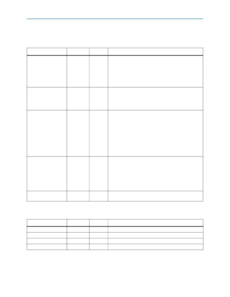
��Table� 3–11.� Memory� Interface� Parameters�
�Parameter�
�Data� bus� width�
�Value�
�≥� 8�
�Units�
�Bits�
�Description�
�The� width� of� your� DDR� or� DDR2� SDRAM� data� interface.� Your� local�
�interface� is� twice� the� width� of� the� memory� interface.� This� value�
�depends� on:�
�■�
�■�
�■�
�The� memory�
�Bandwidth� requirement�
�Number� of� DDIO� pins� available� on� the� selected� FPGA� device�
�Number� of� chip� selects�
�1,� 2,� 4,� or� 8�
�—�
�The� number� of� chip� selects� in� your� memory� interface.� This� is�
�equivalent� to� the� depth� of� your� memory� in� terms� of� number� of�
�chips.� This� value� depends� on� the� type� of� memory� DIMM� selected.�
�If� there� are� two� DIMMs� and� the� memory� modules� on� both� DIMMs�
�have� two� ranks,� the� number� of� chip� selects� is� 4.�
�Number� of� chip� selects�
�per� DIMM�
�1� or� 2�
�—�
�The� number� of� chip� selects� on� each� DIMM� in� your� memory�
�system.� This� option� is� completely� dependent� on� the� type� of�
�external� SDRAM� that� you� are� using.� SDRAMs� may� come� in� two�
�memory� chips� (called� rank)� connected� in� parallel,� with� only� a�
�unique� chip� enable� signal.� This� configuration� allows� the� two� ranks�
�to� share� address� and� data� lines.� Selectively� asserting� only� one�
�chip� enable� signal� at� a� time,� allows� twice� the� memory� depth�
�compared� with� only� a� single� chip.�
�If� there� are� two� memory� chips� in� the� memory� module,� select� 2,�
�otherwise� select� 1.�
�Use� dedicated� PLL�
�outputs�
�On� or� off�
�—�
�Turn� on� to� use� dedicated� PLL� outputs� to� generate� the� clocks,�
�which� is� recommended� for� HardCopy� II� devices.�
�HardCopy� II� designs� use� dedicated� PLL� outputs� for� noise�
�immunity,� better� signal� integrity,� and� minimal� variation� over�
�process,� temperature,� and� voltage.�
�When� turned� off,� the� ALTDDIO� megafunction� generates� the� clock�
�outputs.�
�Number� of� clock� pairs�
�from� FPGA� to� memory�
�1� to� 6�
�—�
�The� number� of� differential� clock� pairs� driven� from� the� FPGA� to� the�
�memory.� More� clock� pairs� reduce� the� loading� of� each� output.�
��Table� 3–12.� Memory� Property� Parameters� (Part� 1� of� 2)�
��Parameter�
�Row� address� bits�
�Column� address� bits�
�Bank� address� bits�
�Precharge� address� bit�
�Range�
�10� to� 14�
�8� to� 13�
�2� or� 3�
�8� or� 10�
�Units�
�Bits�
�Bits�
�Bits�
�–�
�Description�
�The� number� of� row� address� bits� for� your� memory.�
�The� number� of� column� address� bits� for� your� memory.�
�The� number� of� bank� address� bits� for� your� memory.�
�The� address� bit� to� use� as� the� precharge� pin.�
��?� March� 2009� Altera� Corporation�
�相关PDF资料 |
PDF描述 |
|---|---|
| GEM31DTBN-S189 | CONN EDGECARD 62POS R/A .156 SLD |
| GEM31DTBH-S189 | CONN EDGECARD 62POS R/A .156 SLD |
| GEM31DTBD-S189 | CONN EDGECARD 62POS R/A .156 SLD |
| GEM31DTAN-S189 | CONN EDGECARD 62POS R/A .156 SLD |
| 10YXJ2200M10X20 | CAP ALUM 2200UF 10V 20% RADIAL |
相关代理商/技术参数 |
参数描述 |
|---|---|
| IP-RSENC | 功能描述:开发软件 Reed-Solomon Encoder MegaCore RoHS:否 制造商:Atollic Inc. 产品:Compilers/Debuggers 用于:ARM7, ARM9, Cortex-A, Cortex-M, Cortex-R Processors |
| IPR-SLITE2 | 功能描述:开发软件 SerialLite II MegaCore RENEWAL RoHS:否 制造商:Atollic Inc. 产品:Compilers/Debuggers 用于:ARM7, ARM9, Cortex-A, Cortex-M, Cortex-R Processors |
| IPR-SRAM/QDRII | 功能描述:开发软件 QDRII SRAM Control MegaCore RENEWAL RoHS:否 制造商:Atollic Inc. 产品:Compilers/Debuggers 用于:ARM7, ARM9, Cortex-A, Cortex-M, Cortex-R Processors |
| IPR-SSIP | 功能描述:开发软件 Crypto Bundle BU Solution RoHS:否 制造商:Atollic Inc. 产品:Compilers/Debuggers 用于:ARM7, ARM9, Cortex-A, Cortex-M, Cortex-R Processors |
| IPR-TRIETHERNET | 功能描述:开发软件 Triple Speed Ethernt MegaCore RENEWAL RoHS:否 制造商:Atollic Inc. 产品:Compilers/Debuggers 用于:ARM7, ARM9, Cortex-A, Cortex-M, Cortex-R Processors |
发布紧急采购,3分钟左右您将得到回复。