参数资料
| 型号: | W631GG6KB-12 |
| 厂商: | Winbond Electronics |
| 文件页数: | 107/159页 |
| 文件大小: | 0K |
| 描述: | IC DDR3 SDRAM 1GBIT 96WBGA |
| 标准包装: | 200 |
| 格式 - 存储器: | RAM |
| 存储器类型: | DDR3 SDRAM |
| 存储容量: | 1G(64M x 16) |
| 速度: | 800MHz |
| 接口: | 并联 |
| 电源电压: | 1.425 V ~ 1.575 V |
| 工作温度: | 0°C ~ 85°C |
| 封装/外壳: | 96-TFBGA |
| 供应商设备封装: | 96-WBGA(9x13) |
| 包装: | 托盘 |
第1页第2页第3页第4页第5页第6页第7页第8页第9页第10页第11页第12页第13页第14页第15页第16页第17页第18页第19页第20页第21页第22页第23页第24页第25页第26页第27页第28页第29页第30页第31页第32页第33页第34页第35页第36页第37页第38页第39页第40页第41页第42页第43页第44页第45页第46页第47页第48页第49页第50页第51页第52页第53页第54页第55页第56页第57页第58页第59页第60页第61页第62页第63页第64页第65页第66页第67页第68页第69页第70页第71页第72页第73页第74页第75页第76页第77页第78页第79页第80页第81页第82页第83页第84页第85页第86页第87页第88页第89页第90页第91页第92页第93页第94页第95页第96页第97页第98页第99页第100页第101页第102页第103页第104页第105页第106页当前第107页第108页第109页第110页第111页第112页第113页第114页第115页第116页第117页第118页第119页第120页第121页第122页第123页第124页第125页第126页第127页第128页第129页第130页第131页第132页第133页第134页第135页第136页第137页第138页第139页第140页第141页第142页第143页第144页第145页第146页第147页第148页第149页第150页第151页第152页第153页第154页第155页第156页第157页第158页第159页
�� �
�
�W631GG6KB�
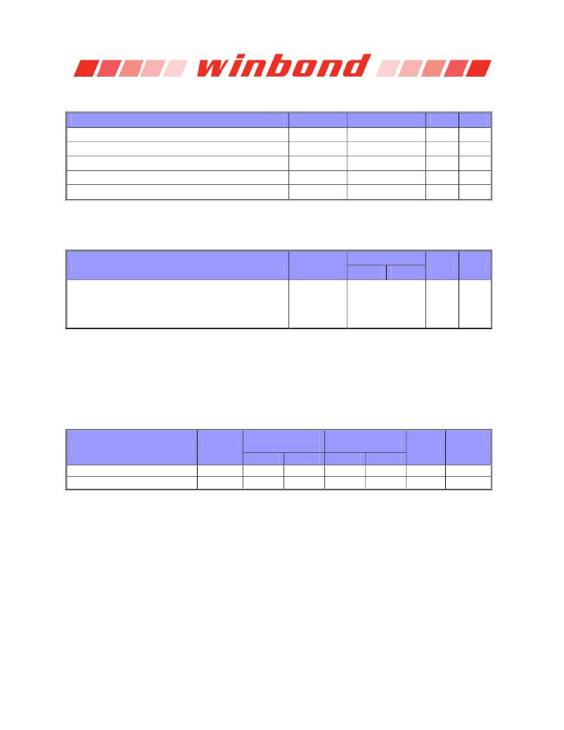
�10.7� DC� and� AC� Output� Measurement� Levels�
�Table� 24� –� Single-ended� DC� and� AC� Output� Levels�
�PARAMETER�
�DC output high measurement level (for IV curve linearity)�
�DC� output� mid� measurement� level� (for� IV� curve� linearity)�
�DC� output� low� measurement� level� (for� IV� curve� linearity)�
�AC� output� high� measurement� level� (for� output� slew� rate)�
�AC� output� low� measurement� level� (for� output� slew� rate)�
�SYMBOL�
�V� OH(DC)�
�V� OM(DC)�
�V� OL(DC)�
�V� OH(AC)�
�V� OL(AC)�
�VALUE�
�0.8� x� V� DDQ�
�0.5� x� V� DDQ�
�0.2� x� V� DDQ�
�V� TT� +� 0.1� x� V� DDQ�
�V� TT� -� 0.1� x� V� DDQ�
�UNIT�
�V�
�V�
�V�
�V�
�V�
�NOTES�
�1�
�1�
�Note:�
�1.� The� swing� of� ±� 0.1� ×� V� DDQ� is� based� on� approximately� 50%� of� the� static� single-ended� output� high� or� low� swing� with� a�
�driver� impedance� of� 34� Ω� and� an� effective� test� load� of� 25� Ω� to� V� TT� =� V� DDQ� /2.�
�Table� 25� –� Differential� DC� and� AC� Output� Levels�
�PARAMETER�
�AC� differential� output� high� measurement� level� (for� output�
�slew� rate)�
�AC� differential� output� low� measurement� level� (for� output�
�slew� rate)�
�SYMBOL�
�V� OH.DIFF(AC)�
�V� OL.DIFF(AC)�
�VALUE�
�MIN.� MAX.�
�+0.2� x� V� DDQ�
�-0.2� x� V� DDQ�
�UNIT�
�V�
�V�
�NOTES�
�1�
�1�
�Note:�
�1.� The� swing� of� ±� 0.2� ×� V� DDQ� is� based� on� approximately� 50%� of� the� static� single-ended� output� high� or� low� swing� with� a�
�driver� impedance� of� 34� Ω� and� an� effective� test� load� of� 25� Ω� to� V� TT� =� V� DDQ� /2� at� each� of� the� differential� outputs.�
�10.7.1� Output� Slew� Rate� Definition� and� Requirements�
�The� slew� rate� definition� depends� if� the� signal� is� single-ended� or� differential.� For� the� relevant� AC� output�
�reference� levels� see� above� Table� 24� and� Table� 25.�
�Table� 26� –� Output� Slew� Rate�
�PARAMETER�
�SYMBOL�
�DDR3-1333,�
�DDR3-1600�
�MIN.�
�MAX.�
�DDR3-1866�
�MIN.�
�MAX.�
�UNIT�
�NOTES�
�Single-ended� Output� Slew� Rate�
�Differential� Output� Slew� Rate�
�SRQse�
�SRQdiff�
�2.5�
�5�
�5�
�10�
�2.5�
�5�
�5*� 1�
�12�
�V/nS�
�V/nS�
�1,� 2,� 3�
�2,� 3�
�Notes:�
�1.� In� two� cases,� a� maximum� slew� rate� of� 6� V/nS� applies� for� a� single� DQ� signal� within� a� byte� lane.�
�-� Case� 1� is� defined� for� a� single� DQ� signal� within� a� byte� lane� which� is� switching� into� a� certain� direction� (either� from� high�
�to� low� or� low� to� high)� while� all� remaining� DQ� signals� in� the� same� byte� lane� are� static� (i.e� they� stay� at� either� high� or� low).�
�-� Case� 2� is� defined� for� a� single� DQ� signal� within� a� byte� lane� which� is� switching� into� a� certain� direction� (either� from� high�
�to� low� or� low� to� high)� while� all� remaining� DQ� signals� in� the� same� byte� lane� are� switching� into� the� opposite� direction� (i.e.�
�from� low� to� high� or� high� to� low� respectively).� For� the� remaining� DQ� signal� switching� into� the� opposite� direction,� the�
�regular� maximum� limit� of� 5� V/nS� applies.�
�2.� Background� for� Symbol� Nomenclature:� SR:� Slew� Rate;� Q:� Query� Output� (like� in� DQ,� which� stands� for� Data-in,� Query-�
�Output);� se:� Single-ended� Signals;� diff:� Differential� Signals.�
�3.� For� R� ON� =� RZQ/7� settings� only.�
�Publication� Release� Date:� Dec.� 09,� 2013�
�Revision� A05�
�-� 107� -�
�相关PDF资料 |
PDF描述 |
|---|---|
| AMC20DRAS-S734 | CONN EDGECARD 40POS .100 R/A PCB |
| FMC12DREI-S13 | CONN EDGECARD 24POS .100 EXTEND |
| EPF6024AQC240-2N | IC FLEX 6000 FPGA 24K 240-PQFP |
| EPF6024AQC240-2 | IC FLEX 6000 FPGA 24K 240-PQFP |
| EPF10K10QC208-3 | IC FLEX 10K FPGA 10K 208-PQFP |
相关代理商/技术参数 |
参数描述 |
|---|---|
| W631GG6KB-15 | 功能描述:IC DDR3 SDRAM 1GBIT 96WBGA RoHS:是 类别:集成电路 (IC) >> 存储器 系列:- 标准包装:2,500 系列:- 格式 - 存储器:EEPROMs - 串行 存储器类型:EEPROM 存储容量:1K (128 x 8) 速度:100kHz 接口:UNI/O?(单线) 电源电压:1.8 V ~ 5.5 V 工作温度:-40°C ~ 85°C 封装/外壳:8-TSSOP,8-MSOP(0.118",3.00mm 宽) 供应商设备封装:8-MSOP 包装:带卷 (TR) |
| W631GG8KB-11 | 制造商:Winbond Electronics Corp 功能描述:IC DDR3 SDRAM 1GBIT 制造商:Winbond Electronics Corp 功能描述:IC DDR3 SDRAM 1GBIT 78WBGA |
| W631GG8KB-12 | 制造商:Winbond Electronics Corp 功能描述:DRAM Chip DDR3 SDRAM 1G-Bit 128Mx8 1.5V 制造商:Winbond Electronics Corp 功能描述:IC DDR3 SDRAM 1GBIT 制造商:Winbond Electronics Corp 功能描述:IC DDR3 SDRAM 1GBIT 78WBGA |
| W631GG8KB-15 | 制造商:Winbond Electronics Corp 功能描述:IC DDR3 SDRAM 1GBIT 制造商:Winbond Electronics Corp 功能描述:IC DDR3 SDRAM 1GBIT 78WBGA |
| W632 | 制造商:LUMINIS 制造商全称:LUMINIS 功能描述:Wall mount |
发布紧急采购,3分钟左右您将得到回复。