参数资料
| 型号: | W631GG6KB-12 |
| 厂商: | Winbond Electronics |
| 文件页数: | 45/159页 |
| 文件大小: | 0K |
| 描述: | IC DDR3 SDRAM 1GBIT 96WBGA |
| 标准包装: | 200 |
| 格式 - 存储器: | RAM |
| 存储器类型: | DDR3 SDRAM |
| 存储容量: | 1G(64M x 16) |
| 速度: | 800MHz |
| 接口: | 并联 |
| 电源电压: | 1.425 V ~ 1.575 V |
| 工作温度: | 0°C ~ 85°C |
| 封装/外壳: | 96-TFBGA |
| 供应商设备封装: | 96-WBGA(9x13) |
| 包装: | 托盘 |
第1页第2页第3页第4页第5页第6页第7页第8页第9页第10页第11页第12页第13页第14页第15页第16页第17页第18页第19页第20页第21页第22页第23页第24页第25页第26页第27页第28页第29页第30页第31页第32页第33页第34页第35页第36页第37页第38页第39页第40页第41页第42页第43页第44页当前第45页第46页第47页第48页第49页第50页第51页第52页第53页第54页第55页第56页第57页第58页第59页第60页第61页第62页第63页第64页第65页第66页第67页第68页第69页第70页第71页第72页第73页第74页第75页第76页第77页第78页第79页第80页第81页第82页第83页第84页第85页第86页第87页第88页第89页第90页第91页第92页第93页第94页第95页第96页第97页第98页第99页第100页第101页第102页第103页第104页第105页第106页第107页第108页第109页第110页第111页第112页第113页第114页第115页第116页第117页第118页第119页第120页第121页第122页第123页第124页第125页第126页第127页第128页第129页第130页第131页第132页第133页第134页第135页第136页第137页第138页第139页第140页第141页第142页第143页第144页第145页第146页第147页第148页第149页第150页第151页第152页第153页第154页第155页第156页第157页第158页第159页
�� �
�
�W631GG6KB�
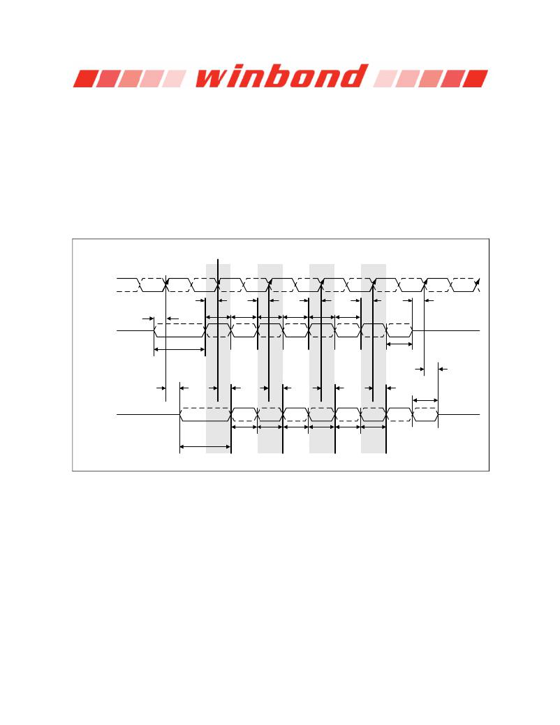
�8.13.2.1� READ� Timing;� Clock� to� Data� Strobe� relationship�
�Clock� to� Data� Strobe� relationship� is� shown� in� Figure� 24� and� is� applied� when� the� DLL� is� enabled� and�
�locked.�
�Rising� data� strobe� edge� parameters:�
�?�
�?�
�?�
�t� DQSCK� min/max� describes� the� allowed� range� for� a� rising� data� strobe� edge� relative� to� CK,� CK#.�
�t� DQSCK� is� the� actual� position� of� a� rising� strobe� edge� relative� to� CK,� CK#.�
�t� QSH� describes� the� data� strobe� high� pulse� width.�
�Falling� data� strobe� edge� parameters:�
�?�
�t� QSL� describes� the� data� strobe� low� pulse� width.�
�t� LZ(DQS)� ,� t� HZ(DQS)� for� preamble/postamble� (see� section� 8.13.2.3� and� Figure� 26).�
�RL� Measured�
�to� this� point�
�CK/CK#�
�t� DQSCK� (min)�
�t� DQSCK� (min)�
�t� DQSCK� (min)�
�t� DQSCK� (min)�
�t� HZ(DQS)� min�
�t� LZ(DQS)� min�
�t� QSH�
�t� QSL�
�t� QSH�
�t� QSL�
�t� QSH�
�t� QSL�
�DQS,� DQS#�
�Erly� Strobe�
�t� RPRE�
�t� RPST�
�Bit� 0�
�Bit� 1�
�Bit� 2�
�Bit� 3�
�Bit� 4�
�Bit� 5�
�Bit� 6�
�Bit� 7�
�t� HZ(DQS)� max�
�t� DQSCK� (max)�
�t� DQSCK� (max)�
�t� DQSCK� (max)�
�t� DQSCK� (max)�
�t� LZ(DQS)� max�
�t� RPST�
�DQS,� DQS#�
�Late� Strobe�
�t� QSH�
�t� QSL�
�t� QSH�
�t� QSL�
�t� QSH�
�t� QSL�
�t� RPRE�
�Bit� 0�
�Bit� 1�
�Bit� 2�
�Bit� 3�
�Bit� 4�
�Bit� 5�
�Bit� 6�
�Bit� 7�
�Notes:�
�1.� Within� a� burst,� rising� strobe� edge� is� not� necessarily� fixed� to� be� always� at� t� DQSCK� (min)� or� t� DQSCK� (max).� Instead,� rising� strobe�
�edge� can� vary� between� t� DQSCK� (min)� and� t� DQSCK� (max).�
�2.� Not� with� standing� note� 1,� a� rising� strobe� edge� with� t� DQSCK� (max)� at� T(n)� can� not� be� immediately� followed� by� a� rising� strobe�
�edge� with� t� DQSCK� (min)� at� T(n+1).� This� is� because� other� timing� relationships� (t� QSH� ,� t� QSL� )� exist:�
�if� t� DQSCK� (n+1)� <� 0:�
�t� DQSCK� (n)� <� 1.0� t� CK� -� (t� QSH� min� +� t� QSL� min)� -� |� t� DQSCK� (n+1)� |�
�3.� The� DQS,� DQS#� differential� output� high� time� is� defined� by� t� QSH� and� the� DQS,� DQS#� differential� output� low� time� is� defined� by�
�t� QSL� .�
�4.� Likewise,� t� LZ(DQS)� min� and� t� HZ(DQS)� min� are� not� tied� to� t� DQSCK,� min� (early� strobe� case)� and� t� LZ(DQS)� max� and� t� HZ(DQS)� max�
�are� not� tied� to� t� DQSCK,� max� (late� strobe� case).�
�5.� The� minimum� pulse� width� of� read� preamble� is� defined� by� t� RPRE� (min).�
�6.� The� maximum� read� postamble� is� bound� by� t� DQSCK� (min)� plus� t� QSH� (min)� on� the� left� side� and� t� HZDSQ� (max)� on� the� right� side.�
�7.� The� minimum� pulse� width� of� read� postamble� is� defined� by� t� RPST� (min).�
�8.� The� maximum� read� preamble� is� bound� by� t� LZDQS� (min)� on� the� left� side� and� t� DQSCK� (max)� on� the� right� side.�
�Figure� 24� –� Clock� to� Data� Strobe� Relationship�
�Publication� Release� Date:� Dec.� 09,� 2013�
�Revision� A05�
�-� 45� -�
�相关PDF资料 |
PDF描述 |
|---|---|
| AMC20DRAS-S734 | CONN EDGECARD 40POS .100 R/A PCB |
| FMC12DREI-S13 | CONN EDGECARD 24POS .100 EXTEND |
| EPF6024AQC240-2N | IC FLEX 6000 FPGA 24K 240-PQFP |
| EPF6024AQC240-2 | IC FLEX 6000 FPGA 24K 240-PQFP |
| EPF10K10QC208-3 | IC FLEX 10K FPGA 10K 208-PQFP |
相关代理商/技术参数 |
参数描述 |
|---|---|
| W631GG6KB-15 | 功能描述:IC DDR3 SDRAM 1GBIT 96WBGA RoHS:是 类别:集成电路 (IC) >> 存储器 系列:- 标准包装:2,500 系列:- 格式 - 存储器:EEPROMs - 串行 存储器类型:EEPROM 存储容量:1K (128 x 8) 速度:100kHz 接口:UNI/O?(单线) 电源电压:1.8 V ~ 5.5 V 工作温度:-40°C ~ 85°C 封装/外壳:8-TSSOP,8-MSOP(0.118",3.00mm 宽) 供应商设备封装:8-MSOP 包装:带卷 (TR) |
| W631GG8KB-11 | 制造商:Winbond Electronics Corp 功能描述:IC DDR3 SDRAM 1GBIT 制造商:Winbond Electronics Corp 功能描述:IC DDR3 SDRAM 1GBIT 78WBGA |
| W631GG8KB-12 | 制造商:Winbond Electronics Corp 功能描述:DRAM Chip DDR3 SDRAM 1G-Bit 128Mx8 1.5V 制造商:Winbond Electronics Corp 功能描述:IC DDR3 SDRAM 1GBIT 制造商:Winbond Electronics Corp 功能描述:IC DDR3 SDRAM 1GBIT 78WBGA |
| W631GG8KB-15 | 制造商:Winbond Electronics Corp 功能描述:IC DDR3 SDRAM 1GBIT 制造商:Winbond Electronics Corp 功能描述:IC DDR3 SDRAM 1GBIT 78WBGA |
| W632 | 制造商:LUMINIS 制造商全称:LUMINIS 功能描述:Wall mount |
发布紧急采购,3分钟左右您将得到回复。