参数资料
| 型号: | W631GG6KB-12 |
| 厂商: | Winbond Electronics |
| 文件页数: | 69/159页 |
| 文件大小: | 0K |
| 描述: | IC DDR3 SDRAM 1GBIT 96WBGA |
| 标准包装: | 200 |
| 格式 - 存储器: | RAM |
| 存储器类型: | DDR3 SDRAM |
| 存储容量: | 1G(64M x 16) |
| 速度: | 800MHz |
| 接口: | 并联 |
| 电源电压: | 1.425 V ~ 1.575 V |
| 工作温度: | 0°C ~ 85°C |
| 封装/外壳: | 96-TFBGA |
| 供应商设备封装: | 96-WBGA(9x13) |
| 包装: | 托盘 |
第1页第2页第3页第4页第5页第6页第7页第8页第9页第10页第11页第12页第13页第14页第15页第16页第17页第18页第19页第20页第21页第22页第23页第24页第25页第26页第27页第28页第29页第30页第31页第32页第33页第34页第35页第36页第37页第38页第39页第40页第41页第42页第43页第44页第45页第46页第47页第48页第49页第50页第51页第52页第53页第54页第55页第56页第57页第58页第59页第60页第61页第62页第63页第64页第65页第66页第67页第68页当前第69页第70页第71页第72页第73页第74页第75页第76页第77页第78页第79页第80页第81页第82页第83页第84页第85页第86页第87页第88页第89页第90页第91页第92页第93页第94页第95页第96页第97页第98页第99页第100页第101页第102页第103页第104页第105页第106页第107页第108页第109页第110页第111页第112页第113页第114页第115页第116页第117页第118页第119页第120页第121页第122页第123页第124页第125页第126页第127页第128页第129页第130页第131页第132页第133页第134页第135页第136页第137页第138页第139页第140页第141页第142页第143页第144页第145页第146页第147页第148页第149页第150页第151页第152页第153页第154页第155页第156页第157页第158页第159页
�� �
�
�W631GG6KB�
�8.17� Power-Down� Modes�
�8.17.1� Power-Down� Entry� and� Exit�
�Power-down� is� synchronously� entered� when� CKE� is� registered� low� (along� with� NOP� or� Deselect�
�command).� CKE� is� not� allowed� to� go� low� while� mode� register� set� command,� MPR� operations,� ZQCAL�
�operations,� DLL� locking� or� read� /� write� operation� are� in� progress.� CKE� is� allowed� to� go� low� while� any�
�of� other� operations� such� as� row� activation,� precharge� or� auto-precharge� and� refresh� are� in� progress,�
�but� power-down� I� DD� spec� will� not� be� applied� until� finishing� those� operations.� Timing� diagrams� are�
�shown� in� Figure� 59� through� Figure� 71� with� details� for� entry� and� exit� of� Power-Down.�
�The� DLL� should� be� in� a� locked� state� when� power-down� is� entered� for� fastest� power-down� exit� timing.� If�
�the� DLL� is� not� locked� during� power-down� entry,� the� DLL� must� be� reset� after� exiting� power-down� mode�
�for� proper� read� operation� and� synchronous� ODT� operation.� DRAM� design� provides� all� AC� and� DC�
�timing� and� voltage� specification� as� well� as� proper� DLL� operation� with� any� CKE� intensive� operations� as�
�long� as� DRAM� controller� complies� with� DRAM� specifications.�
�During� Power-Down,� if� all� banks� are� closed� after� any� in-progress� commands� are� completed,� the�
�device� will� be� in� precharge� Power-Down� mode;� if� any� bank� is� open� after� in-progress� commands� are�
�completed,� the� device� will� be� in� active� Power-Down� mode.�
�Entering� power-down� deactivates� the� input� and� output� buffers,� excluding� CK,� CK#,� ODT,� CKE� and�
�RESET#.� To� protect� DRAM� internal� delay� on� CKE� line� to� block� the� input� signals,� multiple� NOP� or�
�Deselect� commands� are� needed� during� the� CKE� switch� off� and� cycle(s)� after,� this� timing� period� are�
�defined� as� t� CPDED� .� CKE_low� will� result� in� deactivation� of� command� and� address� receivers� after� t� CPDED�
�has� expired.�
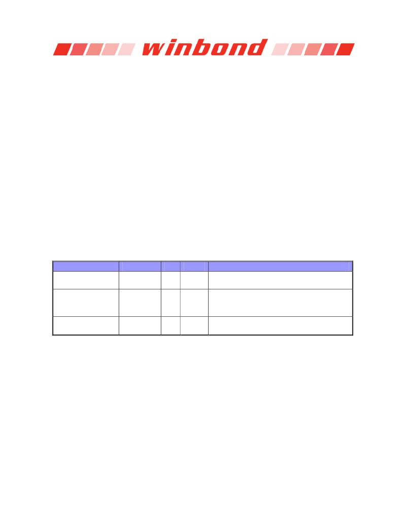
�Table� 7� –� Power-Down� Entry� Definitions�
�Status� of� DRAM�
�Active�
�(A� bank� or� more� Open)�
�Precharged�
�(All� banks� Precharged)�
�Precharged�
�(All� banks� Precharged)�
�MRS� bit� A12�
�Don't� Care�
�0�
�1�
�DLL�
�On�
�Off�
�On�
�PD� Exit�
�Fast�
�Slow�
�Fast�
�Relevant� Parameters�
�tXP� to� any� valid� command�
�tXP� to� any� valid� command.� Since� it� is� in� precharge� state,�
�commands� here� will� be� ACT,� REF,� MRS,� PRE� or� PREA.�
�tXPDLL� to� commands� that� need� the� DLL� to� operate,� such�
�as� RD,� RDA� or� ODT� control� line.�
�tXP� to� any� valid� command�
�Also,� the� DLL� is� disabled� upon� entering� precharge� power-down� (Slow� Exit� Mode),� but� the� DLL� is� kept�
�enabled� during� precharge� power-down� (Fast� Exit� Mode)� or� active� power-down.� In� power-down� mode,�
�CKE� low,� RESET#� high,� and� a� stable� clock� signal� must� be� maintained� at� the� inputs� of� the� DDR3�
�SDRAM,� and� ODT� should� be� in� a� valid� state,� but� all� other� input� signa� ls� are� ―D� on't� Care� .‖� (If� RESET#�
�goes� low� during� Power-Down,� the� DRAM� will� be� out� of� PD� mode� and� into� reset� state.)� CKE� low� must�
�be� maintained� until� t� CKE� has� been� satisfied.� Power-down� duration� is� limited� by� 9� times� t� REFI� of� the�
�device.�
�The� power-down� state� is� synchronously� exited� when� CKE� is� registered� high� (along� with� a� NOP� or�
�Deselect� command).� CKE� high� must� be� maintained� until� t� CKE� has� been� satisfied.� A� valid,� executable�
�command� can� be� applied� with� power-down� exit� latency,� t� XP� and/or� t� XPDLL� after� CKE� goes� high.� Power-�
�down� exit� latency� is� defined� in� section� 10.16� “� AC� Characteristics� ”� on� page� 138.�
�Active� Power� Down� Entry� and� Exit� timing� diagram� example� is� shown� in� Figure� 59.� Timing� Diagrams�
�for� CKE� with� PD� Entry,� PD� Exit� with� Read� and� Read� with� Auto� Precharge,� Write,� Write� with� Auto�
�Precharge,� Activate,� Precharge,� Refresh,� and� MRS� are� shown� in� Figure� 60� through� Figure� 68.�
�Additional� clarifications� are� shown� in� Figure� 69� through� Figure� 71.�
�Publication� Release� Date:� Dec.� 09,� 2013�
�Revision� A05�
�-� 69� -�
�相关PDF资料 |
PDF描述 |
|---|---|
| AMC20DRAS-S734 | CONN EDGECARD 40POS .100 R/A PCB |
| FMC12DREI-S13 | CONN EDGECARD 24POS .100 EXTEND |
| EPF6024AQC240-2N | IC FLEX 6000 FPGA 24K 240-PQFP |
| EPF6024AQC240-2 | IC FLEX 6000 FPGA 24K 240-PQFP |
| EPF10K10QC208-3 | IC FLEX 10K FPGA 10K 208-PQFP |
相关代理商/技术参数 |
参数描述 |
|---|---|
| W631GG6KB-15 | 功能描述:IC DDR3 SDRAM 1GBIT 96WBGA RoHS:是 类别:集成电路 (IC) >> 存储器 系列:- 标准包装:2,500 系列:- 格式 - 存储器:EEPROMs - 串行 存储器类型:EEPROM 存储容量:1K (128 x 8) 速度:100kHz 接口:UNI/O?(单线) 电源电压:1.8 V ~ 5.5 V 工作温度:-40°C ~ 85°C 封装/外壳:8-TSSOP,8-MSOP(0.118",3.00mm 宽) 供应商设备封装:8-MSOP 包装:带卷 (TR) |
| W631GG8KB-11 | 制造商:Winbond Electronics Corp 功能描述:IC DDR3 SDRAM 1GBIT 制造商:Winbond Electronics Corp 功能描述:IC DDR3 SDRAM 1GBIT 78WBGA |
| W631GG8KB-12 | 制造商:Winbond Electronics Corp 功能描述:DRAM Chip DDR3 SDRAM 1G-Bit 128Mx8 1.5V 制造商:Winbond Electronics Corp 功能描述:IC DDR3 SDRAM 1GBIT 制造商:Winbond Electronics Corp 功能描述:IC DDR3 SDRAM 1GBIT 78WBGA |
| W631GG8KB-15 | 制造商:Winbond Electronics Corp 功能描述:IC DDR3 SDRAM 1GBIT 制造商:Winbond Electronics Corp 功能描述:IC DDR3 SDRAM 1GBIT 78WBGA |
| W632 | 制造商:LUMINIS 制造商全称:LUMINIS 功能描述:Wall mount |
发布紧急采购,3分钟左右您将得到回复。