- 您现在的位置:买卖IC网 > PDF目录296802 > PH28F128W18BD60A (INTEL CORP) 8M X 16 FLASH 1.8V PROM, 60 ns, PBGA56 PDF资料下载
参数资料
| 型号: | PH28F128W18BD60A |
| 厂商: | INTEL CORP |
| 元件分类: | PROM |
| 英文描述: | 8M X 16 FLASH 1.8V PROM, 60 ns, PBGA56 |
| 封装: | 9 X 11 MM, 1 MM HEIGHT, LEAD FREE, VFBGA-56 |
| 文件页数: | 56/106页 |
| 文件大小: | 1496K |
| 代理商: | PH28F128W18BD60A |
第1页第2页第3页第4页第5页第6页第7页第8页第9页第10页第11页第12页第13页第14页第15页第16页第17页第18页第19页第20页第21页第22页第23页第24页第25页第26页第27页第28页第29页第30页第31页第32页第33页第34页第35页第36页第37页第38页第39页第40页第41页第42页第43页第44页第45页第46页第47页第48页第49页第50页第51页第52页第53页第54页第55页当前第56页第57页第58页第59页第60页第61页第62页第63页第64页第65页第66页第67页第68页第69页第70页第71页第72页第73页第74页第75页第76页第77页第78页第79页第80页第81页第82页第83页第84页第85页第86页第87页第88页第89页第90页第91页第92页第93页第94页第95页第96页第97页第98页第99页第100页第101页第102页第103页第104页第105页第106页
Intel
Wireless Flash Memory (W18)
Datasheet
Intel Wireless Flash Memory (W18)
07-Dec-2005
Order Number: 290701, Revision: 015
53
9.0
Bus Operations Overview
This section provides an overview of device bus operations. The Intel
Wireless Flash Memory
(W18) family includes an on-chip WSM to manage block erase and program algorithms. Its
Command User Interface (CUI) allows minimal processor overhead with RAM-like interface
timings. Device commands are written to the CUI using standard microprocessor timings.
9.1
Bus Operations
Bus cycles to/from the W18 device conform to standard microprocessor bus operations. Table 18
summarizes the bus operations and the logic levels that must be applied to the device’s control
signal inputs.
9.1.1
Reads
Device read operations are performed by placing the desired address on A[22:0] and asserting CE#
and OE#. ADV# must be low, and WE# and RST# must be high. All read operations are
independent of the voltage level on VPP.
CE#-low selects the device and enables its internal circuits. OE#-low or WE#-low determine
whether DQ[15:0] are outputs or inputs, respectively. OE# and WE# must not be low at the same
time - indeterminate device operation will result.
In asynchronous-page mode, the rising edge of ADV# can be used to latch the address. If only
asynchronous read mode is used, ADV# can be tied to ground. CLK is not used in asynchronous-
page mode and should be tied high.
In synchronous-burst mode, ADV# is used to latch the initial address - either on the rising edge of
ADV# or the rising (or falling) edge of CLK with ADV# low, whichever occurs first. CLK is used
in synchronous-burst mode to increment the internal address counter, and to output read data on
DQ[15:0].
Each device partition can be placed in any of several read states:
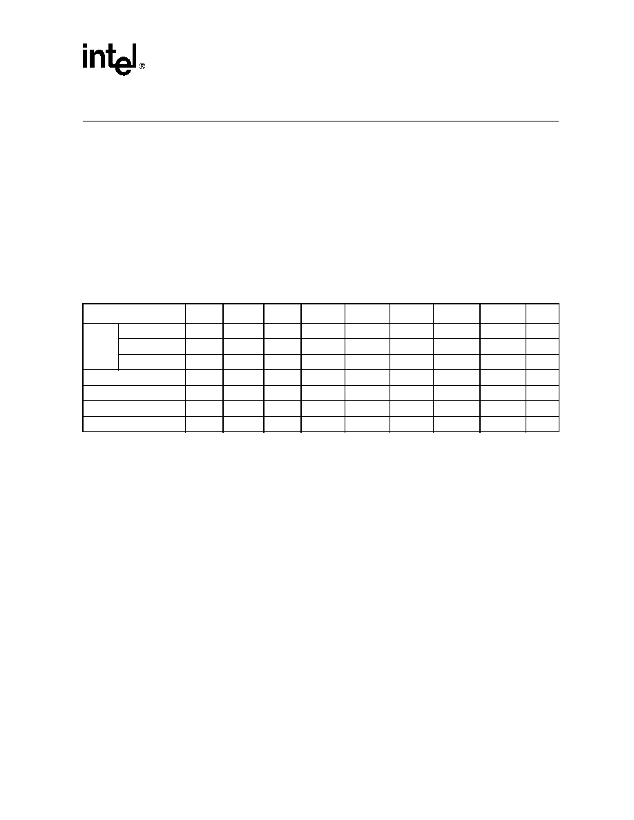
Table 18.
Bus Operations Summary
Bus Operation
RST#
CLK
ADV#
CE#
OE#
WE#
WAIT
DQ[15:0]
Notes
Read
Asynchronous
VIH
X
L
H
Asserted
Output
Synchronous
VIH
Running
L
H
Driven
Output
1
Burst Suspend
VIH
Halted
X
L
H
Active
Output
Write
VIH
X
L
H
L
Asserted
Input
Output Disable
VIH
X
L
H
Asserted
High-Z
Standby
VIH
X
H
X
High-Z
Reset
VIL
X
High-Z
Notes:
1.
WAIT is only valid during synchronous array-read operations.
2.
Refer to the Table 20, “Bus Cycle Definitions” on page 58 for valid DQ[15:0] during a write operation.
3.
X = Don’t Care (H or L).
4.
RST# must be at VSS ± 0.2 V to meet the maximum specified power-down current.
相关PDF资料 |
PDF描述 |
|---|---|
| PHC0683E1133-H | IC SOCKET |
| PHP12NQ15T | N-channel TrenchMOS transistor |
| PHB12NQ15T | N-channel TrenchMOS transistor |
| PHD12NQ15T | N-channel TrenchMOS transistor |
| PHP15N06E | PowerMOS transistor |
相关代理商/技术参数 |
参数描述 |
|---|---|
| PH28F160C3BD70A | 制造商:Micron Technology Inc 功能描述:MM#865392FLASH 28F160C3BD 70 VF-PBGA46 C |
| PH28F256L18B85 | 制造商:INTEL 制造商全称:Intel Corporation 功能描述:StrataFlash Wireless Memory |
| PH28F256L18B85A | 制造商:Micron Technology Inc 功能描述:MM#875138FLASH 28F256L18B 85 VF-PBGA79 S |
| PH28F256L18T85 | 制造商:INTEL 制造商全称:Intel Corporation 功能描述:StrataFlash Wireless Memory |
| PH28F320C3TD70A | 制造商:Micron Technology Inc 功能描述:Flash Mem Parallel 3V/3.3V 32M-Bit 2M x 16 70ns 48-Pin VFBGA Tray 制造商:Micron Technology Inc 功能描述:MM#869664FLASH 28F320C3TD 70 VF-PBGA47 E |
发布紧急采购,3分钟左右您将得到回复。