- 您现在的位置:买卖IC网 > PDF目录67672 > GT-96100A (Galileo Technology Services, LLC) Advanced Communication Controller That Handles a Wide Range of Serial Communication Protocols,such as Ethernet,Fast Ethernet,and HDLC(通信协议的高级通信协议(以太网、快速以太网、HDLC)控制器) PDF资料下载
参数资料
| 型号: | GT-96100A |
| 厂商: | Galileo Technology Services, LLC |
| 英文描述: | Advanced Communication Controller That Handles a Wide Range of Serial Communication Protocols,such as Ethernet,Fast Ethernet,and HDLC(通信协议的高级通信协议(以太网、快速以太网、HDLC)控制器) |
| 中文描述: | 先进的通信控制器能够处理的串行通信协议,范围广,如以太网,快速以太网,和HDLC(通信协议的高级通信协议(以太网,快速以太网,HDLC的)控制器) |
| 文件页数: | 212/549页 |
| 文件大小: | 7321K |
| 代理商: | GT-96100A |
第1页第2页第3页第4页第5页第6页第7页第8页第9页第10页第11页第12页第13页第14页第15页第16页第17页第18页第19页第20页第21页第22页第23页第24页第25页第26页第27页第28页第29页第30页第31页第32页第33页第34页第35页第36页第37页第38页第39页第40页第41页第42页第43页第44页第45页第46页第47页第48页第49页第50页第51页第52页第53页第54页第55页第56页第57页第58页第59页第60页第61页第62页第63页第64页第65页第66页第67页第68页第69页第70页第71页第72页第73页第74页第75页第76页第77页第78页第79页第80页第81页第82页第83页第84页第85页第86页第87页第88页第89页第90页第91页第92页第93页第94页第95页第96页第97页第98页第99页第100页第101页第102页第103页第104页第105页第106页第107页第108页第109页第110页第111页第112页第113页第114页第115页第116页第117页第118页第119页第120页第121页第122页第123页第124页第125页第126页第127页第128页第129页第130页第131页第132页第133页第134页第135页第136页第137页第138页第139页第140页第141页第142页第143页第144页第145页第146页第147页第148页第149页第150页第151页第152页第153页第154页第155页第156页第157页第158页第159页第160页第161页第162页第163页第164页第165页第166页第167页第168页第169页第170页第171页第172页第173页第174页第175页第176页第177页第178页第179页第180页第181页第182页第183页第184页第185页第186页第187页第188页第189页第190页第191页第192页第193页第194页第195页第196页第197页第198页第199页第200页第201页第202页第203页第204页第205页第206页第207页第208页第209页第210页第211页当前第212页第213页第214页第215页第216页第217页第218页第219页第220页第221页第222页第223页第224页第225页第226页第227页第228页第229页第230页第231页第232页第233页第234页第235页第236页第237页第238页第239页第240页第241页第242页第243页第244页第245页第246页第247页第248页第249页第250页第251页第252页第253页第254页第255页第256页第257页第258页第259页第260页第261页第262页第263页第264页第265页第266页第267页第268页第269页第270页第271页第272页第273页第274页第275页第276页第277页第278页第279页第280页第281页第282页第283页第284页第285页第286页第287页第288页第289页第290页第291页第292页第293页第294页第295页第296页第297页第298页第299页第300页第301页第302页第303页第304页第305页第306页第307页第308页第309页第310页第311页第312页第313页第314页第315页第316页第317页第318页第319页第320页第321页第322页第323页第324页第325页第326页第327页第328页第329页第330页第331页第332页第333页第334页第335页第336页第337页第338页第339页第340页第341页第342页第343页第344页第345页第346页第347页第348页第349页第350页第351页第352页第353页第354页第355页第356页第357页第358页第359页第360页第361页第362页第363页第364页第365页第366页第367页第368页第369页第370页第371页第372页第373页第374页第375页第376页第377页第378页第379页第380页第381页第382页第383页第384页第385页第386页第387页第388页第389页第390页第391页第392页第393页第394页第395页第396页第397页第398页第399页第400页第401页第402页第403页第404页第405页第406页第407页第408页第409页第410页第411页第412页第413页第414页第415页第416页第417页第418页第419页第420页第421页第422页第423页第424页第425页第426页第427页第428页第429页第430页第431页第432页第433页第434页第435页第436页第437页第438页第439页第440页第441页第442页第443页第444页第445页第446页第447页第448页第449页第450页第451页第452页第453页第454页第455页第456页第457页第458页第459页第460页第461页第462页第463页第464页第465页第466页第467页第468页第469页第470页第471页第472页第473页第474页第475页第476页第477页第478页第479页第480页第481页第482页第483页第484页第485页第486页第487页第488页第489页第490页第491页第492页第493页第494页第495页第496页第497页第498页第499页第500页第501页第502页第503页第504页第505页第506页第507页第508页第509页第510页第511页第512页第513页第514页第515页第516页第517页第518页第519页第520页第521页第522页第523页第524页第525页第526页第527页第528页第529页第530页第531页第532页第533页第534页第535页第536页第537页第538页第539页第540页第541页第542页第543页第544页第545页第546页第547页第548页第549页
GT-96100A Advanced Communication Controller
Revision 1.0
29
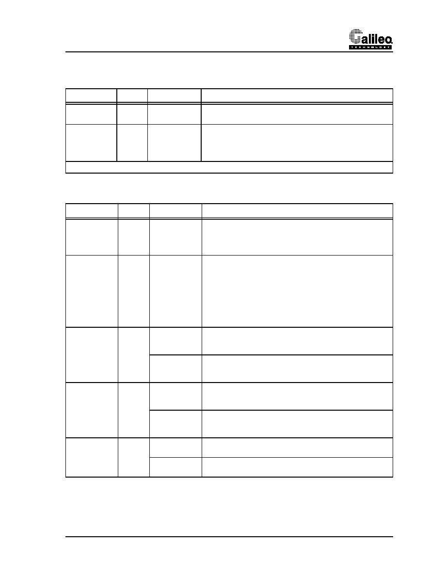
PErr0*
I/O
STS
PCI_0 Parity
Error
Asserted when a data parity error is detected.
This pin features a sustained tristate output.
SErr0*
OD
PCI_0 System
Error
Asserted when a serious system error (not necessarily a PCI_0
error) is detected. SErr0* behavior in the GT-96100A is pro-
grammable (refer to PCI section for details).
This pin features an open-drain output.
PCI Bus 0 Total: 50
Table 7:
PCI Bus 1 Pin Assignments
Pin Name
Type
Full Name
Description
VREF1
I
PCI_1 Voltage
Reference
Must be connected directly to the 3.3V or the 5V power plane
depending on which voltage level PCI_1 supports.
NOTE: VREF0 and VREF1 can be completely independent
voltage levels.
PClk1
I
PCI_1 Clock
Provides the timing for PCI_1 transactions. The PCI_1 clock
range is between 0 and 66MHz.
Runs independently of PClk0.
Active only when PCI _1 is enabled.
NOTE: The PClk0 cycle must be higher than the TClk cycle
by at least 1ns. This clock frequency can be indepen-
dent of both TClk and PClk0. See Section 32.1 “TClk/
PAD1[31:0]/
PAD0[63:32]
I/O
PCI_1
Address/Data
During the first clock of the transaction, PAD1[31:0] contains a
physical byte address (32 bits). During subsequent clock
cycles, PAD1[31:0] contains data.
PCI_0 (64 bit)
Address/Data
If PCI_0 is configured for 64 bit, these pins function as
PAD0[63:32] and carry the most significant 32 bits of data for
PCI_0 transactions.
CBE1[3:0]*/
CBE0[7:4]*
I/O
PCI_1 Com-
mand/Byte
Enable
During the address phase of the transaction, CBE1[3:0]* pro-
vide the PCI_1 bus command. During the data phase, these
lines provide the byte enables.
PCI_0 (64 bit)
Byte Enable
If PCI_0 is configured for 64 bit, these pins function as
CBE0[7:4]* and carry byte enables for the most significant 32
bits of PCI_0 data.
Par1/Par64
I/O
PCI_1 Parity
Calculated by the GT-96100A as an even parity bit for
PAD1[31:0] and CBE1[3:0]* lines.
PCI_0 (64 bit)
Parity
If PCI_0 is configured for 64 bit, this pin functions as Par64 and
carries even parity bit for PAD0[63:32] and CBE0[7:4]*.
Table 6:
PCI Bus 0 Pin Assignments (Continued)
Pin Name
Type
Full Name
Description
相关PDF资料 |
PDF描述 |
|---|---|
| GT5-2/1S-HU | RECTANGULAR CONNECTOR |
| GT5-1S-HU(A) | RECTANGULAR CONNECTOR |
| GT5-1S-HU(B) | RECTANGULAR CONNECTOR |
| GT5-2S-HU | RECTANGULAR CONNECTOR |
| GT5-4S-HU | RECTANGULAR CONNECTOR |
相关代理商/技术参数 |
参数描述 |
|---|---|
| GT96100AB3-BBF-C000 | 制造商:Marvell 功能描述:Marvell GT96100AB3-BBF-C000 |
| GT96100AB3-BBF-C083 | 制造商:Marvell 功能描述:Marvell GT96100AB3-BBF-C083 |
| GT96103AB3-BBF-C083 | 制造商:Marvell 功能描述: 制造商:Marvell 功能描述:Marvell GT96103AB3-BBF-C083 |
| GT96122-A2-BBF1C000 | 制造商:Marvell 功能描述:Marvell GT96122-A2-BBF1C000 |
| GT96122-Ax-BBF-C000 | 制造商:Marvell 功能描述:64-BIT MIPS COMMUNICATION CONTROLLER & INTEGRATED NETGX COPR - Trays |
发布紧急采购,3分钟左右您将得到回复。