- 您现在的位置:买卖IC网 > PDF目录67965 > MC68330FC16 (MOTOROLA INC) 32-BIT, 16.78 MHz, MICROPROCESSOR, PQFP132 PDF资料下载
参数资料
| 型号: | MC68330FC16 |
| 厂商: | MOTOROLA INC |
| 元件分类: | 微控制器/微处理器 |
| 英文描述: | 32-BIT, 16.78 MHz, MICROPROCESSOR, PQFP132 |
| 封装: | PLASTIC, QFP-132 |
| 文件页数: | 124/261页 |
| 文件大小: | 1153K |
| 代理商: | MC68330FC16 |
第1页第2页第3页第4页第5页第6页第7页第8页第9页第10页第11页第12页第13页第14页第15页第16页第17页第18页第19页第20页第21页第22页第23页第24页第25页第26页第27页第28页第29页第30页第31页第32页第33页第34页第35页第36页第37页第38页第39页第40页第41页第42页第43页第44页第45页第46页第47页第48页第49页第50页第51页第52页第53页第54页第55页第56页第57页第58页第59页第60页第61页第62页第63页第64页第65页第66页第67页第68页第69页第70页第71页第72页第73页第74页第75页第76页第77页第78页第79页第80页第81页第82页第83页第84页第85页第86页第87页第88页第89页第90页第91页第92页第93页第94页第95页第96页第97页第98页第99页第100页第101页第102页第103页第104页第105页第106页第107页第108页第109页第110页第111页第112页第113页第114页第115页第116页第117页第118页第119页第120页第121页第122页第123页当前第124页第125页第126页第127页第128页第129页第130页第131页第132页第133页第134页第135页第136页第137页第138页第139页第140页第141页第142页第143页第144页第145页第146页第147页第148页第149页第150页第151页第152页第153页第154页第155页第156页第157页第158页第159页第160页第161页第162页第163页第164页第165页第166页第167页第168页第169页第170页第171页第172页第173页第174页第175页第176页第177页第178页第179页第180页第181页第182页第183页第184页第185页第186页第187页第188页第189页第190页第191页第192页第193页第194页第195页第196页第197页第198页第199页第200页第201页第202页第203页第204页第205页第206页第207页第208页第209页第210页第211页第212页第213页第214页第215页第216页第217页第218页第219页第220页第221页第222页第223页第224页第225页第226页第227页第228页第229页第230页第231页第232页第233页第234页第235页第236页第237页第238页第239页第240页第241页第242页第243页第244页第245页第246页第247页第248页第249页第250页第251页第252页第253页第254页第255页第256页第257页第258页第259页第260页第261页
MOTOROLA
MC68330 USER’S MANUAL
2- 3
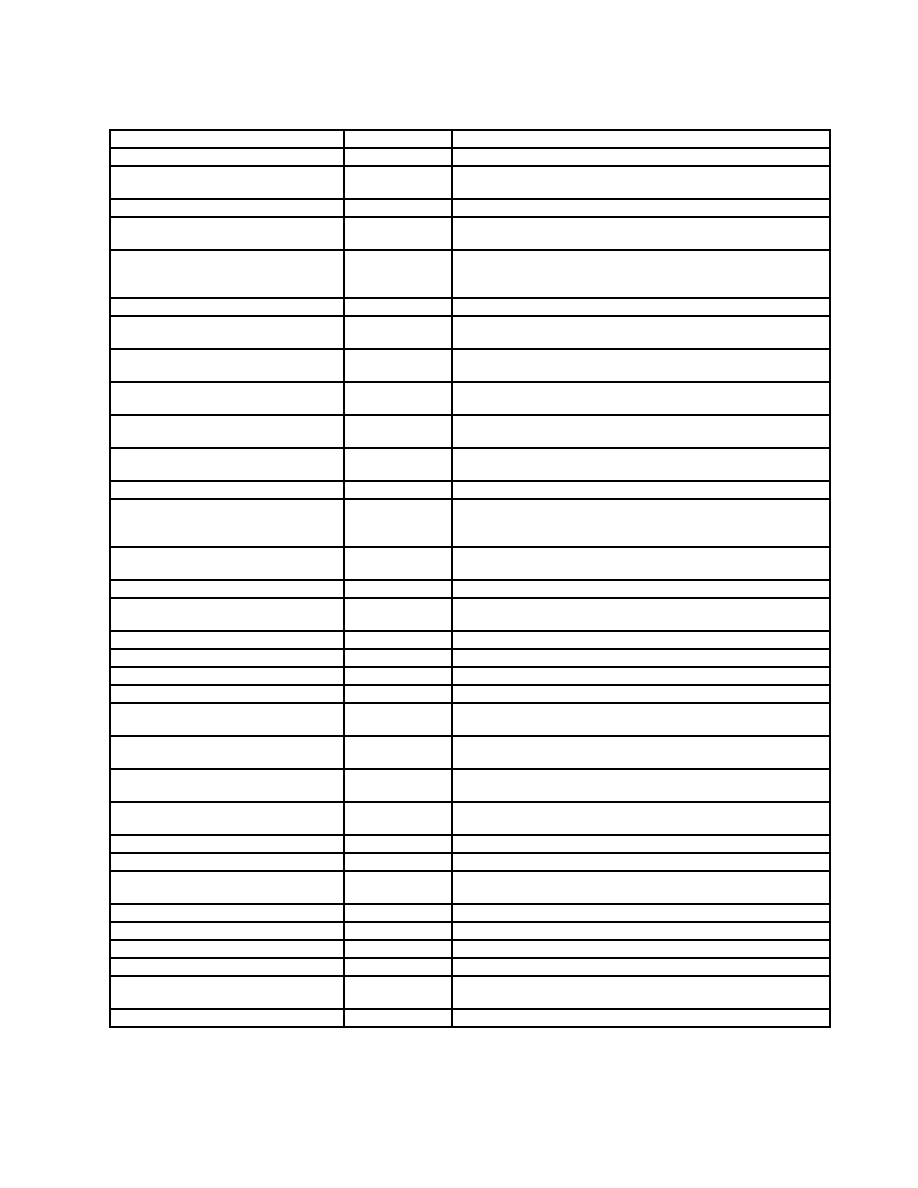
Table 2-1. Signal Index
Signal Name
Mnemonic
Function
Address Bus
A23–A0
Lower 24 bits of address bus
Address Bus/ Port A7–A0/
IACK7–
IACK1
A31–A24
Upper eight bits of address bus, parallel I/O port, or interrupt
acknowledge lines
Data Bus
D15–D0
16-bit data bus used to transfer byte or word data
Function Codes
FC2–FC0
Identifies the processor state and the address space of the
current bus cycle
Chip Select /
AVEC
CS3–
CS0
Enables peripherals at programmed addresses or provides
automatic vector request (
CS0) during an interrupt
acknowledge cycle
Bus Request
BR
Indicates that an external device requires bus mastership
Bus Grant
BG
Indicates that current bus cycle is complete and the
MC68330 has relinquished the bus
Bus Grant Acknowledge
BGACK
Indicates that an external device has assumed bus
mastership
Data and Size Acknowledge
DSACK1,
DSACK0
Provides asynchronous data transfers and dynamic bus
sizing
Byte Write Enable
UWE, LWE
Provides an enable signal for byte writes to external devices,
when using a 16-bit port
Read-Modify-Write Cycle
RMC
Identifies the bus cycle as part of an indivisible read-modify-
write operation
Address Strobe
AS
Indicates that a valid address is on the address bus
Data Strobe
DS
During a read cycle,
DS indicates that an external device
should place valid data on the data bus. During a write cycle,
DS indicates that valid data is on the data bus.
Size
SIZ1, SIZ0
Indicates the number of bytes remaining to be transferred for
this cycle
Read/Write
R/
W
Indicates the direction of data transfer on the bus
Interrupt Request Level/
Port B7 – B1
IRQ7 – IRQ1
Provides an interrupt priority level to the CPU32 or provides
parallel I/O
Reset
RESET
System reset
Halt
HALT
Suspend external bus activity
Bus Error
BERR
Indicates an erroneous bus operation is being attempted
System Clock Out
CLKOUT
Internal system clock output
Crystal Oscillator
EXTAL, XTAL
Connections for an external crystal to the internal oscillator
circuit
External Filter Capacitor
XFC
Connection pin for an external capacitor to filter the circuit of
the phase-locked loop
Clock Mode Select/Port B0
MODCK
Selects the source of the internal system clock or furnishes a
parallel I/O bit
Instruction Fetch
IFETCH
Indicates when the CPU32 is performing an instruction word
prefetch and when the instruction pipeline has been flushed
Instruction Pipe
IPIPE
Tracks movement of words through the instruction pipeline
Breakpoint
BKPT
Signals a hardware breakpoint to the CPU32
Freeze
FREEZE
Indicates that the CPU32 has entered background debug
mode
Test Clock
TCK
Provides a clock for IEEE 1149.1 test logic
Test Mode Select
TMS
Controls test mode operations
Test Data In
TDI
Shifts in test instructions and test data
Test Data Out
TDO
Shifts out test instructions and test data
Synchronizer Power
VCCSYN
Quiet power supply to VCO; also used to control synthesizer
mode after reset.
System Power Supply and Return
VCC, GND
Power supply and return to the MC68330
相关PDF资料 |
PDF描述 |
|---|---|
| MC68332AMPV16 | 32-BIT, 16.78 MHz, MICROCONTROLLER, PQFP144 |
| MC68332GMPV20 | 32-BIT, 20.97 MHz, MICROCONTROLLER, PQFP144 |
| MC68332AVPV16 | 32-BIT, 16.78 MHz, MICROCONTROLLER, PQFP144 |
| MC68332GMPV16 | 32-BIT, 16.78 MHz, MICROCONTROLLER, PQFP144 |
| SPAKMC332GMPV20 | 32-BIT, 20.97 MHz, MICROCONTROLLER, PQFP144 |
相关代理商/技术参数 |
参数描述 |
|---|---|
| MC68330FE16 | 制造商:FREESCALE 制造商全称:Freescale Semiconductor, Inc 功能描述:Integrated CPU32 Processor |
| MC68330FE16V | 制造商:FREESCALE 制造商全称:Freescale Semiconductor, Inc 功能描述:Integrated CPU32 Processor |
| MC68330FE25 | 制造商:FREESCALE 制造商全称:Freescale Semiconductor, Inc 功能描述:Integrated CPU32 Processor |
| MC68330FE8V | 制造商:FREESCALE 制造商全称:Freescale Semiconductor, Inc 功能描述:Integrated CPU32 Processor |
| MC68330FG16 | 制造商:FREESCALE 制造商全称:Freescale Semiconductor, Inc 功能描述:Integrated CPU32 Processor |
发布紧急采购,3分钟左右您将得到回复。