- 您现在的位置:买卖IC网 > PDF目录67965 > MC68330FC16 (MOTOROLA INC) 32-BIT, 16.78 MHz, MICROPROCESSOR, PQFP132 PDF资料下载
参数资料
| 型号: | MC68330FC16 |
| 厂商: | MOTOROLA INC |
| 元件分类: | 微控制器/微处理器 |
| 英文描述: | 32-BIT, 16.78 MHz, MICROPROCESSOR, PQFP132 |
| 封装: | PLASTIC, QFP-132 |
| 文件页数: | 203/261页 |
| 文件大小: | 1153K |
| 代理商: | MC68330FC16 |
第1页第2页第3页第4页第5页第6页第7页第8页第9页第10页第11页第12页第13页第14页第15页第16页第17页第18页第19页第20页第21页第22页第23页第24页第25页第26页第27页第28页第29页第30页第31页第32页第33页第34页第35页第36页第37页第38页第39页第40页第41页第42页第43页第44页第45页第46页第47页第48页第49页第50页第51页第52页第53页第54页第55页第56页第57页第58页第59页第60页第61页第62页第63页第64页第65页第66页第67页第68页第69页第70页第71页第72页第73页第74页第75页第76页第77页第78页第79页第80页第81页第82页第83页第84页第85页第86页第87页第88页第89页第90页第91页第92页第93页第94页第95页第96页第97页第98页第99页第100页第101页第102页第103页第104页第105页第106页第107页第108页第109页第110页第111页第112页第113页第114页第115页第116页第117页第118页第119页第120页第121页第122页第123页第124页第125页第126页第127页第128页第129页第130页第131页第132页第133页第134页第135页第136页第137页第138页第139页第140页第141页第142页第143页第144页第145页第146页第147页第148页第149页第150页第151页第152页第153页第154页第155页第156页第157页第158页第159页第160页第161页第162页第163页第164页第165页第166页第167页第168页第169页第170页第171页第172页第173页第174页第175页第176页第177页第178页第179页第180页第181页第182页第183页第184页第185页第186页第187页第188页第189页第190页第191页第192页第193页第194页第195页第196页第197页第198页第199页第200页第201页第202页当前第203页第204页第205页第206页第207页第208页第209页第210页第211页第212页第213页第214页第215页第216页第217页第218页第219页第220页第221页第222页第223页第224页第225页第226页第227页第228页第229页第230页第231页第232页第233页第234页第235页第236页第237页第238页第239页第240页第241页第242页第243页第244页第245页第246页第247页第248页第249页第250页第251页第252页第253页第254页第255页第256页第257页第258页第259页第260页第261页
3- 18
MC68330 USER’S MANUAL
MOTOROLA
1. NEGATE DS, AS, AND UWE
2. REMOVE DATA FROM D15–
BUS MASTER
SLAVE
ADDRESS DEVICE
1. SET R/W TO WRITE
2. DRIVE ADDRESS ON A31–A0
3. DRIVE FUNCTION CODE ON FC2–FC0
4. DRIVE SIZE PINS FOR OPERAND SIZE
5. ASSERT AS AND UWE/LWE
6. PLACE DATA ON D15–D0
7. ASSERT DS
TERMINATE OUTPUT TRANSFE
START NEXT CYCLE
1. DECODE ADDRESS
2. LATCH DATA FROM D15–D0
ACCEPT DATA
3. ASSERT DSACKx SIGN
TERMINATE CYCLE
1. NEGATE DSAC
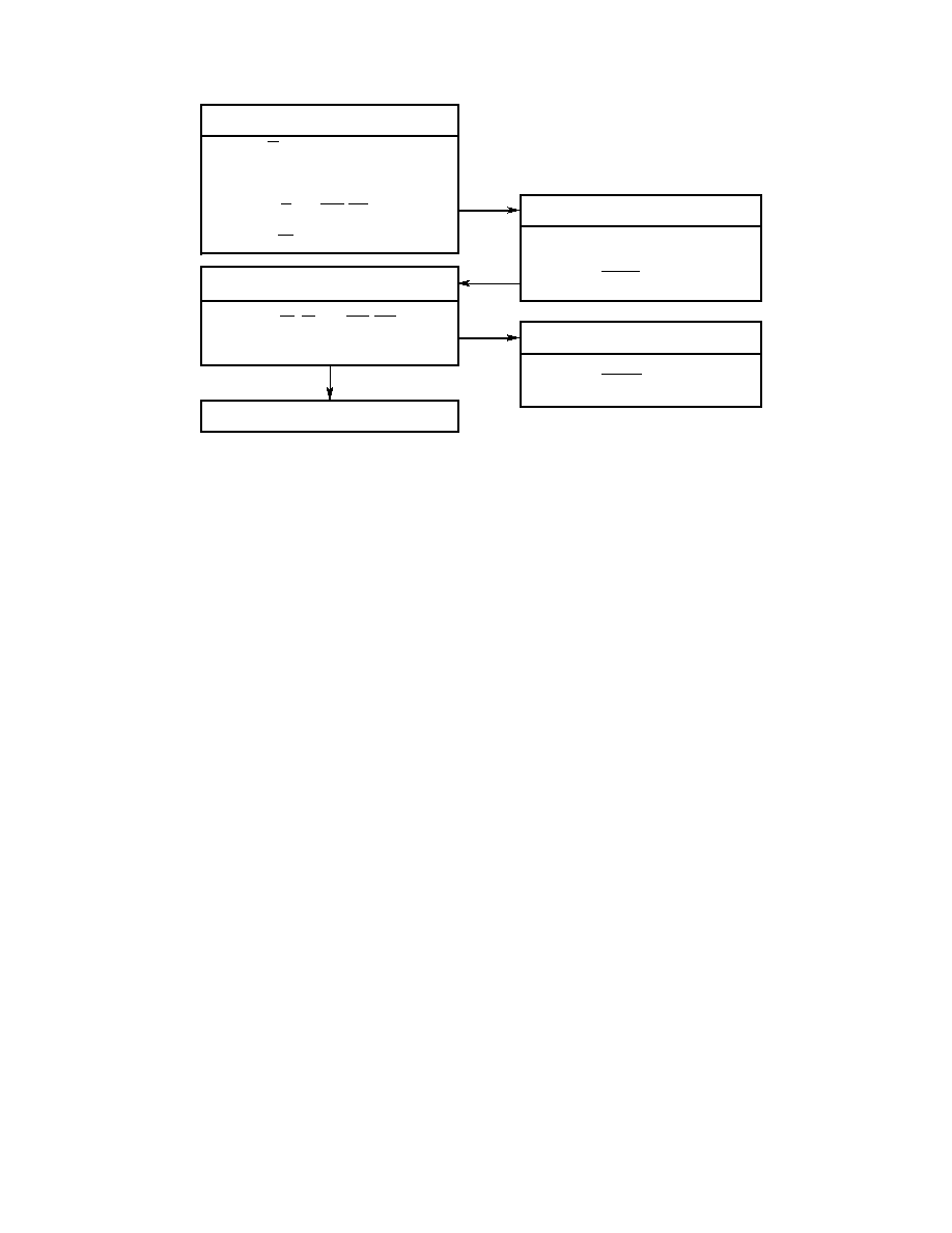
Figure 3-8. Write Cycle Flowchart
State 0 – The write cycle starts in S0. During S0, the MC68330 places a valid address
on A31-A0 and valid function codes on FC2-FC0. The function codes select the
address space for the cycle. The MC68330 drives R/
W low for a write cycle. SIZ1
and SIZ0 become valid, indicating the number of bytes to be transferred.
State 1 – One-half clock later, in S1, the MC68330 asserts
AS, indicating a valid
address on the address bus. During this state
UWE and/or LWE is asserted
simultaneously with
AS.
State 2 – During S2, the MC68330 places the data to be written onto D15-D0, and
samples
DSACKx at the end of S2.
State 3 – The MC68330 asserts
DS during S3, indicating that data is stable on the
data bus. As long as at least one of the
DSACKx signals is recognized by the end
of S2 (meeting the asynchronous input setup time requirement), the cycle
terminates one clock later. If
DSACKx is not recognized by the start of S3, the
MC68330 inserts wait states instead of proceeding to S4 and S5. To ensure that
wait states are inserted, both
DSACK1 and DSACK0 must remain negated
throughout the asynchronous input setup and hold times around the end of S2. If
wait states are added, the MC68330 continues to sample
DSACKx on the falling
edges of the clock until one is recognized. The selected device uses R/
W, SIZ1,
SIZ0, and A0 to latch data from the appropriate byte(s) of D15-D8, and D7-D0.
SIZ1, SIZ0, and A0 select the bytes of the data bus. If it has not already done so,
the device asserts
DSACKx to signal that it has successfully stored the data.
State 4 – The MC68330 issues no new control signals during S4.
State 5 – The MC68330 negates
AS and DS during S5. It holds the address and data
valid during S5 to provide address hold time for memory systems. R/
W, SIZ1, SIZ0,
and FC2-FC0 also remain valid throughout S5. The external device must keep
相关PDF资料 |
PDF描述 |
|---|---|
| MC68332AMPV16 | 32-BIT, 16.78 MHz, MICROCONTROLLER, PQFP144 |
| MC68332GMPV20 | 32-BIT, 20.97 MHz, MICROCONTROLLER, PQFP144 |
| MC68332AVPV16 | 32-BIT, 16.78 MHz, MICROCONTROLLER, PQFP144 |
| MC68332GMPV16 | 32-BIT, 16.78 MHz, MICROCONTROLLER, PQFP144 |
| SPAKMC332GMPV20 | 32-BIT, 20.97 MHz, MICROCONTROLLER, PQFP144 |
相关代理商/技术参数 |
参数描述 |
|---|---|
| MC68330FE16 | 制造商:FREESCALE 制造商全称:Freescale Semiconductor, Inc 功能描述:Integrated CPU32 Processor |
| MC68330FE16V | 制造商:FREESCALE 制造商全称:Freescale Semiconductor, Inc 功能描述:Integrated CPU32 Processor |
| MC68330FE25 | 制造商:FREESCALE 制造商全称:Freescale Semiconductor, Inc 功能描述:Integrated CPU32 Processor |
| MC68330FE8V | 制造商:FREESCALE 制造商全称:Freescale Semiconductor, Inc 功能描述:Integrated CPU32 Processor |
| MC68330FG16 | 制造商:FREESCALE 制造商全称:Freescale Semiconductor, Inc 功能描述:Integrated CPU32 Processor |
发布紧急采购,3分钟左右您将得到回复。