- 您现在的位置:买卖IC网 > PDF目录67965 > MC68330FC16 (MOTOROLA INC) 32-BIT, 16.78 MHz, MICROPROCESSOR, PQFP132 PDF资料下载
参数资料
| 型号: | MC68330FC16 |
| 厂商: | MOTOROLA INC |
| 元件分类: | 微控制器/微处理器 |
| 英文描述: | 32-BIT, 16.78 MHz, MICROPROCESSOR, PQFP132 |
| 封装: | PLASTIC, QFP-132 |
| 文件页数: | 152/261页 |
| 文件大小: | 1153K |
| 代理商: | MC68330FC16 |
第1页第2页第3页第4页第5页第6页第7页第8页第9页第10页第11页第12页第13页第14页第15页第16页第17页第18页第19页第20页第21页第22页第23页第24页第25页第26页第27页第28页第29页第30页第31页第32页第33页第34页第35页第36页第37页第38页第39页第40页第41页第42页第43页第44页第45页第46页第47页第48页第49页第50页第51页第52页第53页第54页第55页第56页第57页第58页第59页第60页第61页第62页第63页第64页第65页第66页第67页第68页第69页第70页第71页第72页第73页第74页第75页第76页第77页第78页第79页第80页第81页第82页第83页第84页第85页第86页第87页第88页第89页第90页第91页第92页第93页第94页第95页第96页第97页第98页第99页第100页第101页第102页第103页第104页第105页第106页第107页第108页第109页第110页第111页第112页第113页第114页第115页第116页第117页第118页第119页第120页第121页第122页第123页第124页第125页第126页第127页第128页第129页第130页第131页第132页第133页第134页第135页第136页第137页第138页第139页第140页第141页第142页第143页第144页第145页第146页第147页第148页第149页第150页第151页当前第152页第153页第154页第155页第156页第157页第158页第159页第160页第161页第162页第163页第164页第165页第166页第167页第168页第169页第170页第171页第172页第173页第174页第175页第176页第177页第178页第179页第180页第181页第182页第183页第184页第185页第186页第187页第188页第189页第190页第191页第192页第193页第194页第195页第196页第197页第198页第199页第200页第201页第202页第203页第204页第205页第206页第207页第208页第209页第210页第211页第212页第213页第214页第215页第216页第217页第218页第219页第220页第221页第222页第223页第224页第225页第226页第227页第228页第229页第230页第231页第232页第233页第234页第235页第236页第237页第238页第239页第240页第241页第242页第243页第244页第245页第246页第247页第248页第249页第250页第251页第252页第253页第254页第255页第256页第257页第258页第259页第260页第261页
MOTOROLA
MC68330 USER’S MANUAL
6-3
To ensure proper operation, the open-drain pins require external pullups. Twenty-one
bits in the boundary scan register define the output enable signal for associated groups
of bidirectional and three-state pins. The 21 control bits and their bit positions are listed
in Table 6-1.
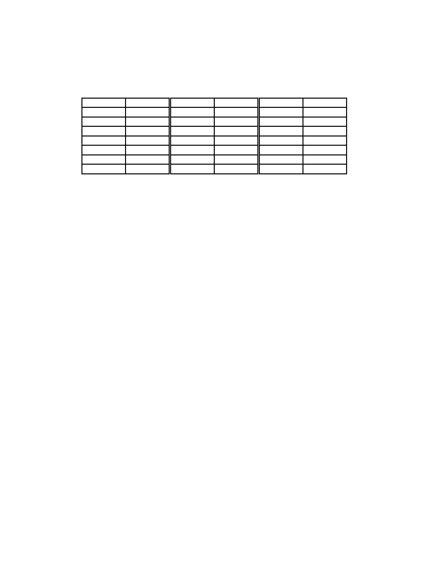
Table 6-1. Boundary Scan Control Bits
Name
Bit Number
Name
Bit Number
Name
Bit Number
cs0.ctl
4
a27.ctl
68
irq7.ctl
95
ifetch.ctl
34
a26.ctl
70
irq6.ctl
97
modck.ctl
39
a25.ctl
72
irq5.ctl
99
a31.ctl
60
a24.ctl
74
irq4.ctl
101
a30.ctl
62
ab.ctl
78
irq3.ctl
103
a29.ctl
64
berr.ctl
79
irq2.ctl
105
a28.ctl
66
db.ctl
80
irq1.ctl
107
Boundary scan bit definitions are shown in Table 6-2. The first column in Table 6-2
defines the bit's ordinal position in the boundary scan register. The shift register cell
nearest TDO (i.e., first to be shifted out) is defined as bit zero; the last bit to be shifted out
is 107.
The second column references one of the five MC68330 cell types depicted in Figures 6-
2 – 6-6, which describe the cell structure for that bit.
The third column lists the pin name for all pin-related cells or defines the name of
bidirectional control register bits. The active level of the control bits (i.e., output driver on)
is defined by the last digit of the cell type listed for each control bit. For example, the
active-high level for ab.ctl (bit 78) is logic one since the cell type is IO.Ctl1. The active
level for cs0.ctl (bit 4) is logic zero, since the cell type is IO.Ctl0. IO.Ctl0 (see Figure 6-5)
differs from IO.Ctl1 (see Figure 6-4) by an inverter in the output enable path.
The fourth column lists the pin type: TS-Output indicates a three-state output pin, I/O
indicates a bidirectional pin, and OD-I/O denotes an open-drain bidirectional pin. An
open-drain output pin has two states: off (high impedance) and logic zero.
The last column indicates the associated boundary scan register control bit for
bidirectional and three-state pins.
Bidirectional pins include a single scan cell for data (IO.Cell) as depicted in Figure 6-6.
These cells are controlled by one of the two cells shown in Figures 6-4 and 6-5. One or
more bidirectional data cells can be serially connected to a control cell as shown in
Figure 6-7. Note that, when sampling the bidirectional data cells, the cell data can be
interpreted only after examining the IO control cell to determine pin direction.
相关PDF资料 |
PDF描述 |
|---|---|
| MC68332AMPV16 | 32-BIT, 16.78 MHz, MICROCONTROLLER, PQFP144 |
| MC68332GMPV20 | 32-BIT, 20.97 MHz, MICROCONTROLLER, PQFP144 |
| MC68332AVPV16 | 32-BIT, 16.78 MHz, MICROCONTROLLER, PQFP144 |
| MC68332GMPV16 | 32-BIT, 16.78 MHz, MICROCONTROLLER, PQFP144 |
| SPAKMC332GMPV20 | 32-BIT, 20.97 MHz, MICROCONTROLLER, PQFP144 |
相关代理商/技术参数 |
参数描述 |
|---|---|
| MC68330FE16 | 制造商:FREESCALE 制造商全称:Freescale Semiconductor, Inc 功能描述:Integrated CPU32 Processor |
| MC68330FE16V | 制造商:FREESCALE 制造商全称:Freescale Semiconductor, Inc 功能描述:Integrated CPU32 Processor |
| MC68330FE25 | 制造商:FREESCALE 制造商全称:Freescale Semiconductor, Inc 功能描述:Integrated CPU32 Processor |
| MC68330FE8V | 制造商:FREESCALE 制造商全称:Freescale Semiconductor, Inc 功能描述:Integrated CPU32 Processor |
| MC68330FG16 | 制造商:FREESCALE 制造商全称:Freescale Semiconductor, Inc 功能描述:Integrated CPU32 Processor |
发布紧急采购,3分钟左右您将得到回复。