- 您现在的位置:买卖IC网 > PDF目录299522 > MT45W2MW16BBB-856WT 2M X 16 PSEUDO STATIC RAM, 85 ns, PBGA54 PDF资料下载
参数资料
| 型号: | MT45W2MW16BBB-856WT |
| 元件分类: | SRAM |
| 英文描述: | 2M X 16 PSEUDO STATIC RAM, 85 ns, PBGA54 |
| 封装: | 6 X 8 MM, 1 MM HEIGHT, 0.75 MM PITCH, LEAD FREE, VFBGA-54 |
| 文件页数: | 13/56页 |
| 文件大小: | 709K |
| 代理商: | MT45W2MW16BBB-856WT |
第1页第2页第3页第4页第5页第6页第7页第8页第9页第10页第11页第12页当前第13页第14页第15页第16页第17页第18页第19页第20页第21页第22页第23页第24页第25页第26页第27页第28页第29页第30页第31页第32页第33页第34页第35页第36页第37页第38页第39页第40页第41页第42页第43页第44页第45页第46页第47页第48页第49页第50页第51页第52页第53页第54页第55页第56页
4 MEG x 16, 2 MEG x 16
ASYNC/PAGE/BURST CellularRAM MEMORY
09005aef80be1fbd pdf/09005aef80be2036 zip
Micron Technology, Inc., reserves the right to change products or specifications without notice.
Burst CellularRAM_2.fm - Rev. D 9/04 EN
20
2003 Micron Technology, Inc. All rights reserved.
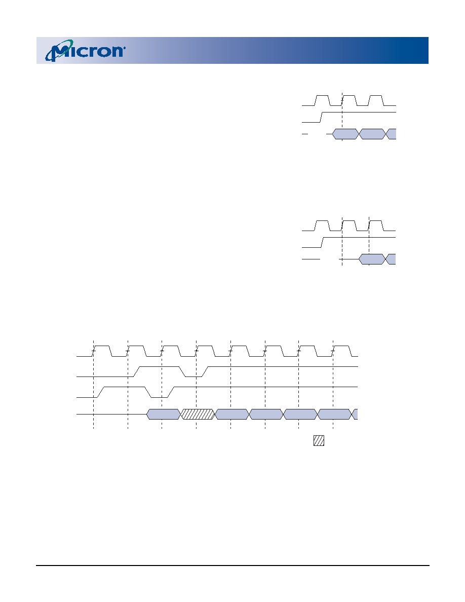
WAIT Configuration (BCR[8])
Default = WAIT Transitions One Clock
Before Data Valid/Invalid
The WAIT configuration bit is used to determine
when WAIT transitions between the asserted and the
de-asserted state with respect to valid data presented
on the data bus. The memory controller will use the
WAIT signal to coordinate data transfer during synchro-
nous READ and WRITE operations. When BCR[8] = 0,
data will be valid or invalid on the clock edge immedi-
ately after WAIT transitions to the de-asserted or
A8 = 1, the WAIT signal transitions one clock period
prior to the data bus going valid or invalid (Figures 18
and 19).
WAIT Polarity (BCR[10])
Default = WAIT Active HIGH
The WAIT polarity bit indicates whether an asserted
WAIT output should be HIGH or LOW. This bit will
determine whether the WAIT signal requires a pull-up
or pull-down resistor to maintain the de-asserted
state.
Figure 17: WAIT Configuration (BCR[8] = 0)
NOTE:
1. Note: Data valid/invalid immediately after WAIT
transitions (BCR[8] = 0). See Figure 19.
Figure 18: WAIT Configuration (BCR[8] = 1)
NOTE:
1. Note: Valid/invalid data delayed for one clock after
WAIT transitions (BCR[8] = 1). See Figure 19.
Figure 19: WAIT Configuration During Burst Operation
NOTE:
1. Non-default BCR setting for WAIT configuration during burst operation: WAIT active LOW.
WAIT
DQ[15:0]
CLK
Data[0]
Data[1]
Data immediately valid (or invalid)
High-Z
WAIT
D[15:0]
CLK
Data[0]
Data valid (or invalid) after one clock delay
High-Z
WAIT
DQ[15:0]
CLK
D[0]
D[1]
BCR[8] = 0
Data valid in current cycle.
BCR[8] = 1
Data valid in next cycle.
DON’T CARE
D[2]
D[3]
D[4]
相关PDF资料 |
PDF描述 |
|---|---|
| MT46H32M32LGCM-5IT:A | 32M X 32 DDR DRAM, 5 ns, PBGA90 |
| MT46HC32M16LFCX-75:B | 32M X 16 DDR DRAM, 7.5 ns, PBGA90 |
| MT46HC32M16LGCM-54IT:B | 32M X 16 DDR DRAM, 5.4 ns, PBGA90 |
| MT47H32M16BT-37VL:A | 32M X 16 DDR DRAM, 0.5 ns, PBGA92 |
| MT47H64M16HQ-3IT:G | 64M X 16 DDR DRAM, 0.4 ns, PBGA60 |
相关代理商/技术参数 |
参数描述 |
|---|---|
| MT45W2MW16BFB-601 WT | 制造商:Micron Technology Inc 功能描述: |
| MT45W2MW16BFB-701 WT | 制造商:Micron Technology Inc 功能描述: |
| MT45W2MW16BFB-706 WT | 制造商:Micron Technology Inc 功能描述:PSRAM ASYNC 1 32MBIT 2MX16 70NS 54VFBGA - Trays |
| MT45W2MW16BFB-708 WT | 制造商:Micron Technology Inc 功能描述:PSRAM ASYNC 1 32MBIT 2MX16 70NS - Trays |
| MT45W2MW16BFB-856 WT | 制造商:Micron Technology Inc 功能描述:PSRAM ASYNC 1 32MBIT 2MX16 85NS 54VFBGA - Trays |
发布紧急采购,3分钟左右您将得到回复。