- 您现在的位置:买卖IC网 > PDF目录299522 > MT45W2MW16BBB-856WT 2M X 16 PSEUDO STATIC RAM, 85 ns, PBGA54 PDF资料下载
参数资料
| 型号: | MT45W2MW16BBB-856WT |
| 元件分类: | SRAM |
| 英文描述: | 2M X 16 PSEUDO STATIC RAM, 85 ns, PBGA54 |
| 封装: | 6 X 8 MM, 1 MM HEIGHT, 0.75 MM PITCH, LEAD FREE, VFBGA-54 |
| 文件页数: | 4/56页 |
| 文件大小: | 709K |
| 代理商: | MT45W2MW16BBB-856WT |
第1页第2页第3页当前第4页第5页第6页第7页第8页第9页第10页第11页第12页第13页第14页第15页第16页第17页第18页第19页第20页第21页第22页第23页第24页第25页第26页第27页第28页第29页第30页第31页第32页第33页第34页第35页第36页第37页第38页第39页第40页第41页第42页第43页第44页第45页第46页第47页第48页第49页第50页第51页第52页第53页第54页第55页第56页
4 MEG x 16, 2 MEG x 16
ASYNC/PAGE/BURST CellularRAM MEMORY
09005aef80be1fbd pdf/09005aef80be2036 zip
Micron Technology, Inc., reserves the right to change products or specifications without notice.
Burst CellularRAM_2.fm - Rev. D 9/04 EN
12
2003 Micron Technology, Inc. All rights reserved.
Mixed-Mode Operation
The device can support a combination of synchro-
nous READ and asynchronous WRITE operations
when the BCR is configured for synchronous opera-
tion. The asynchronous WRITE operation requires that
the clock (CLK) remain static (HIGH or LOW) during
the entire sequence. The ADV# signal can be used to
latch the target address, or it can remain LOW during
the entire WRITE operation. CE# must return HIGH
when transitioning between mixed-mode operations.
Note that the tCKA period is the same as a READ or
WRITE cycle. This time is required to ensure adequate
refresh. Mixed-mode operation facilitates a seamless
interface to legacy burst mode Flash memory control-
lers. See Figure 40 on page 48 for the “Asynchronous
WRITE Followed by Burst READ” timing diagram.
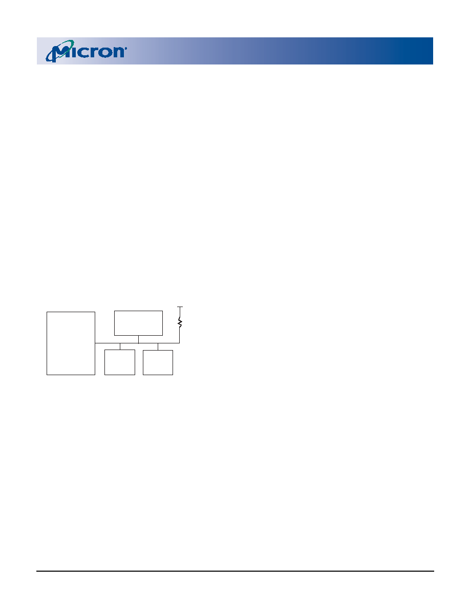
WAIT Operation
The WAIT output on a CellularRAM device is typi-
cally connected to a shared, system-level WAIT signal
(see Figure 9). The shared WAIT signal is used by the
processor to coordinate transactions with multiple
memories on the synchronous bus.
Figure 9: Wired or WAIT Configuration
Once a READ or WRITE operation has been initi-
ated, WAIT goes active to indicate that the Cellular-
RAM device requires additional time before data can
be transferred. For READ operations, WAIT will remain
active until valid data is output from the device. For
WRITE operations, WAIT will indicate to the memory
controller when data will be accepted into the Cellu-
larRAM device. When WAIT transitions to an inactive
state, the data burst will progress on successive clock
edges.
CE# must remain asserted during WAIT cycles
(WAIT asserted and WAIT configuration BCR[8] = 1).
Bringing CE# HIGH during WAIT cycles may cause
data corruption. (Note that for BCR[8] = 0, the actual
WAIT cycles end one cycle after WAIT de-asserts, and
for row boundary crossings, start one cycle after the
WAIT signal asserts.)
The WAIT output also performs an arbitration role
when a READ or WRITE operation is launched while
an on-chip refresh is in progress. If a collision occurs,
WAIT is asserted for additional clock cycles until the
page 13). When the refresh operation has completed,
the READ or WRITE operation will continue normally.
WAIT is also asserted when a continuous READ or
WRITE burst crosses a row boundary. The WAIT asser-
tion allows time for the new row to be accessed, and
permits any pending refresh operations to be per-
formed.
LB#/UB# Operation
The LB# enable and UB# enable signals support
byte-wide data transfers. During READ operations, the
enabled byte(s) are driven onto the DQs. The DQs
associated with a disabled byte are put into a High-Z
state during a READ operation. During WRITE opera-
tions, any disabled bytes will not be transferred to the
RAM array and the internal value will remain
unchanged. During an asynchronous WRITE cycle, the
data to be written is latched on the rising edge of CE#,
WE#, LB#, or UB#, whichever occurs first.
When both the LB# and UB# are disabled (HIGH)
during an operation, the device will disable the data
bus from receiving or transmitting data. Although the
device will seem to be deselected, it remains in an
active mode as long as CE# remains LOW.
CellularRAM
External
Pull-Up/
Pull-Down
Resistor
Processor
READY
Other
Device
WAIT
Other
Device
WAIT
相关PDF资料 |
PDF描述 |
|---|---|
| MT46H32M32LGCM-5IT:A | 32M X 32 DDR DRAM, 5 ns, PBGA90 |
| MT46HC32M16LFCX-75:B | 32M X 16 DDR DRAM, 7.5 ns, PBGA90 |
| MT46HC32M16LGCM-54IT:B | 32M X 16 DDR DRAM, 5.4 ns, PBGA90 |
| MT47H32M16BT-37VL:A | 32M X 16 DDR DRAM, 0.5 ns, PBGA92 |
| MT47H64M16HQ-3IT:G | 64M X 16 DDR DRAM, 0.4 ns, PBGA60 |
相关代理商/技术参数 |
参数描述 |
|---|---|
| MT45W2MW16BFB-601 WT | 制造商:Micron Technology Inc 功能描述: |
| MT45W2MW16BFB-701 WT | 制造商:Micron Technology Inc 功能描述: |
| MT45W2MW16BFB-706 WT | 制造商:Micron Technology Inc 功能描述:PSRAM ASYNC 1 32MBIT 2MX16 70NS 54VFBGA - Trays |
| MT45W2MW16BFB-708 WT | 制造商:Micron Technology Inc 功能描述:PSRAM ASYNC 1 32MBIT 2MX16 70NS - Trays |
| MT45W2MW16BFB-856 WT | 制造商:Micron Technology Inc 功能描述:PSRAM ASYNC 1 32MBIT 2MX16 85NS 54VFBGA - Trays |
发布紧急采购,3分钟左右您将得到回复。