- 您现在的位置:买卖IC网 > PDF目录299522 > MT45W2MW16BBB-856WT 2M X 16 PSEUDO STATIC RAM, 85 ns, PBGA54 PDF资料下载
参数资料
| 型号: | MT45W2MW16BBB-856WT |
| 元件分类: | SRAM |
| 英文描述: | 2M X 16 PSEUDO STATIC RAM, 85 ns, PBGA54 |
| 封装: | 6 X 8 MM, 1 MM HEIGHT, 0.75 MM PITCH, LEAD FREE, VFBGA-54 |
| 文件页数: | 15/56页 |
| 文件大小: | 709K |
| 代理商: | MT45W2MW16BBB-856WT |
第1页第2页第3页第4页第5页第6页第7页第8页第9页第10页第11页第12页第13页第14页当前第15页第16页第17页第18页第19页第20页第21页第22页第23页第24页第25页第26页第27页第28页第29页第30页第31页第32页第33页第34页第35页第36页第37页第38页第39页第40页第41页第42页第43页第44页第45页第46页第47页第48页第49页第50页第51页第52页第53页第54页第55页第56页
4 MEG x 16, 2 MEG x 16
ASYNC/PAGE/BURST CellularRAM MEMORY
09005aef80be1fbd pdf/09005aef80be2036 zip
Micron Technology, Inc., reserves the right to change products or specifications without notice.
Burst CellularRAM_2.fm - Rev. D 9/04 EN
22
2003 Micron Technology, Inc. All rights reserved.
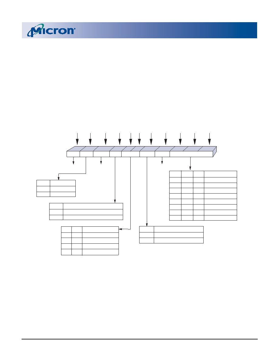
Refresh Configuration Register
The refresh configuration register (RCR) defines
how the CellularRAM device performs its transparent
self refresh. Altering the refresh parameters can dra-
matically reduce current consumption during standby
mode. Page mode control is also embedded into the
RCR. Figure 21 describes the control bits used in the
RCR. At power-up, the RCR is set to 0070h.
The RCR is accessed using CRE and A[19] LOW; or
through the configuration register software access
sequence with DQ = 0000h on the third cycle (see
Partial Array Refresh (RCR[2:0])
Default = Full Array Refresh
The PAR bits restrict refresh operation to a portion
of the total memory array. This feature allows the
device to reduce standby current by refreshing only
that part of the memory array required by the host sys-
tem. The refresh options are full array, one-half array,
one-quarter array, one-eighth array, or none of the
array. The mapping of these partitions can start at
either the beginning or the end of the address map
Figure 21: Refresh Configuration Register Mapping
PAR
A4
A3
A2
A1
A0
Read Configuration
Register
Address Bus
4
5
1
2
3
0
RESERVED
6
A5
0
1
Deep Power-Down
DPD Enable
DPD Disable (default)
RCR[4]
TCR
RCR[6] RCR[5]
1
0
Maximum Case Temp.
+85C (default)
+70C
+45C
+15C
A6
All must be set to "0"
A[18:8]
18–8
19
21–20
Register
Select
RESERVED
A[21:20]
A19
0
1
Register Select
Select RCR
Select BCR
RCR[19]
All must be set to "0"
RCR[1]
0
1
RCR[0]
0
1
0
1
Refresh Coverage
Full array (default)
Bottom 1/2 array
Bottom 1/4 array
Bottom 1/8 array
RCR[2]
0
00
1
0
1
0
1
11
1
None of array
Top 1/2 array
Top 1/4 array
Top 1/8 array
DPD
Must be set to "0"
A7
7
PAGE
0
1
Page Mode Enable/Disable
Page Mode Disabled (default)
Page Mode Enable
RCR[7]
相关PDF资料 |
PDF描述 |
|---|---|
| MT46H32M32LGCM-5IT:A | 32M X 32 DDR DRAM, 5 ns, PBGA90 |
| MT46HC32M16LFCX-75:B | 32M X 16 DDR DRAM, 7.5 ns, PBGA90 |
| MT46HC32M16LGCM-54IT:B | 32M X 16 DDR DRAM, 5.4 ns, PBGA90 |
| MT47H32M16BT-37VL:A | 32M X 16 DDR DRAM, 0.5 ns, PBGA92 |
| MT47H64M16HQ-3IT:G | 64M X 16 DDR DRAM, 0.4 ns, PBGA60 |
相关代理商/技术参数 |
参数描述 |
|---|---|
| MT45W2MW16BFB-601 WT | 制造商:Micron Technology Inc 功能描述: |
| MT45W2MW16BFB-701 WT | 制造商:Micron Technology Inc 功能描述: |
| MT45W2MW16BFB-706 WT | 制造商:Micron Technology Inc 功能描述:PSRAM ASYNC 1 32MBIT 2MX16 70NS 54VFBGA - Trays |
| MT45W2MW16BFB-708 WT | 制造商:Micron Technology Inc 功能描述:PSRAM ASYNC 1 32MBIT 2MX16 70NS - Trays |
| MT45W2MW16BFB-856 WT | 制造商:Micron Technology Inc 功能描述:PSRAM ASYNC 1 32MBIT 2MX16 85NS 54VFBGA - Trays |
发布紧急采购,3分钟左右您将得到回复。