- 您现在的位置:买卖IC网 > PDF目录299522 > MT45W2MW16BBB-856WT 2M X 16 PSEUDO STATIC RAM, 85 ns, PBGA54 PDF资料下载
参数资料
| 型号: | MT45W2MW16BBB-856WT |
| 元件分类: | SRAM |
| 英文描述: | 2M X 16 PSEUDO STATIC RAM, 85 ns, PBGA54 |
| 封装: | 6 X 8 MM, 1 MM HEIGHT, 0.75 MM PITCH, LEAD FREE, VFBGA-54 |
| 文件页数: | 56/56页 |
| 文件大小: | 709K |
| 代理商: | MT45W2MW16BBB-856WT |
第1页第2页第3页第4页第5页第6页第7页第8页第9页第10页第11页第12页第13页第14页第15页第16页第17页第18页第19页第20页第21页第22页第23页第24页第25页第26页第27页第28页第29页第30页第31页第32页第33页第34页第35页第36页第37页第38页第39页第40页第41页第42页第43页第44页第45页第46页第47页第48页第49页第50页第51页第52页第53页第54页第55页当前第56页
4 MEG x 16, 2 MEG x 16
ASYNC/PAGE/BURST CellularRAM MEMORY
09005aef80be1fbd pdf/09005aef80be2036 zip
Micron Technology, Inc., reserves the right to change products or specifications without notice.
Burst CellularRAM_2.fm - Rev. D 9/04 EN
9
2003 Micron Technology, Inc. All rights reserved.
Functional Description
In general, the MT45W4MW16BFB device and the
MT45W2MW16BFB device are high-density alterna-
tives to SRAM and Pseudo SRAM products, popular in
low-power, portable applications.
The MT45W4MW16BFB device contains 67,108,864
bits organized as 4,194,304 addresses by 16 bits. The
MT45W2MW16BFB contains 33,554,432 bits organized
as 2,097,152 addresses by 16 bits. Both devices imple-
ment the same high-speed bus interface found on
burst mode Flash products.
The CellularRAM bus interface supports both asyn-
chronous and burst mode transfers. Page mode
accesses are also included as a bandwidth-enhancing
extension to the asynchronous read protocol.
Power-Up Initialization
CellularRAM products include an on-chip voltage
sensor used to launch the power-up initialization pro-
cess. Initialization will configure the BCR and the RCR
with their default settings (see Table 16 on page 18 and
simultaneously. When they reach a stable level at or
above 1.70V, the device will require 150s to complete
its self-initialization process. During the initialization
period, CE# should remain HIGH. When initialization
is complete, the device is ready for normal operation.
Figure 3: Power-Up Initialization
Timing
Bus Operating Modes
The MT45W4MW16BFB and MT45W2MW16BFB
CellularRAM products incorporate a burst mode inter-
face found on Flash products targeting low-power,
wireless applications. This bus interface supports
asynchronous, page mode, and burst mode read and
write transfers. The specific interface supported is
defined by the value loaded into the BCR. Page mode is
controlled by the refresh configuration register
(RCR[7]).
Asynchronous Mode
CellularRAM products power up in the asynchro-
nous operating mode. This mode uses the industry-
standard SRAM control bus (CE#, OE#, WE#, LB#/
UB#). READ operations (Figure 4) are initiated by
bringing CE#, OE#, and LB#/UB# LOW while keeping
WE# HIGH. Valid data will be driven out of the I/Os
after the specified access time has elapsed. WRITE
operations (Figure 5) occur when CE#, WE#, and LB#/
UB# are driven LOW. During asynchronous WRITE
operations, the OE# level is a “Don't Care,” and WE#
will override OE#. The data to be written is latched on
the rising edge of CE#, WE#, or LB#/UB# (whichever
occurs first). Asynchronous operations (page mode
disabled) can either use the ADV input to latch the
address, or ADV can be driven LOW during the entire
READ/WRITE operation.
During asynchronous operation, the CLK input must
be static (HIGH or LOW—no transitions). WAIT will be
driven while the device is enabled and its state should
be ignored. WE# LOW time must be limited to tCEM.
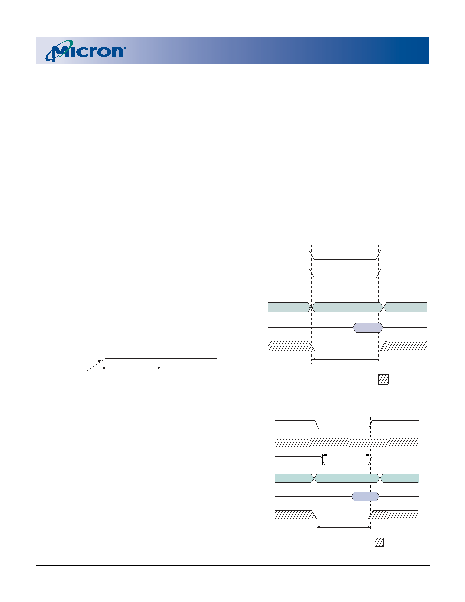
Figure 4: READ Operation (ADV = LOW)
NOTE: ADV must remain LOW for page mode operation
.
Figure 5: WRITE Operation (ADV = LOW)
Vcc
VccQ
Device Initialization
Vcc = 1.70V
Device ready for
normal operation
tPU > 150s
ADDRESS VALID
DATA
CE#
DON’T CARE
DATA VALID
OE#
WE#
LB#/UB#
tRC = READ Cycle Time
ADDRESS
ADDRESS VALID
< tCEM
DATA
CE#
DON’T CARE
DATA VALID
OE#
WE#
LB#/UB#
tWC = WRITE Cycle Time
ADDRESS
相关PDF资料 |
PDF描述 |
|---|---|
| MT46H32M32LGCM-5IT:A | 32M X 32 DDR DRAM, 5 ns, PBGA90 |
| MT46HC32M16LFCX-75:B | 32M X 16 DDR DRAM, 7.5 ns, PBGA90 |
| MT46HC32M16LGCM-54IT:B | 32M X 16 DDR DRAM, 5.4 ns, PBGA90 |
| MT47H32M16BT-37VL:A | 32M X 16 DDR DRAM, 0.5 ns, PBGA92 |
| MT47H64M16HQ-3IT:G | 64M X 16 DDR DRAM, 0.4 ns, PBGA60 |
相关代理商/技术参数 |
参数描述 |
|---|---|
| MT45W2MW16BFB-601 WT | 制造商:Micron Technology Inc 功能描述: |
| MT45W2MW16BFB-701 WT | 制造商:Micron Technology Inc 功能描述: |
| MT45W2MW16BFB-706 WT | 制造商:Micron Technology Inc 功能描述:PSRAM ASYNC 1 32MBIT 2MX16 70NS 54VFBGA - Trays |
| MT45W2MW16BFB-708 WT | 制造商:Micron Technology Inc 功能描述:PSRAM ASYNC 1 32MBIT 2MX16 70NS - Trays |
| MT45W2MW16BFB-856 WT | 制造商:Micron Technology Inc 功能描述:PSRAM ASYNC 1 32MBIT 2MX16 85NS 54VFBGA - Trays |
发布紧急采购,3分钟左右您将得到回复。