- 您现在的位置:买卖IC网 > PDF目录299522 > MT45W2MW16BBB-856WT 2M X 16 PSEUDO STATIC RAM, 85 ns, PBGA54 PDF资料下载
参数资料
| 型号: | MT45W2MW16BBB-856WT |
| 元件分类: | SRAM |
| 英文描述: | 2M X 16 PSEUDO STATIC RAM, 85 ns, PBGA54 |
| 封装: | 6 X 8 MM, 1 MM HEIGHT, 0.75 MM PITCH, LEAD FREE, VFBGA-54 |
| 文件页数: | 9/56页 |
| 文件大小: | 709K |
| 代理商: | MT45W2MW16BBB-856WT |
第1页第2页第3页第4页第5页第6页第7页第8页当前第9页第10页第11页第12页第13页第14页第15页第16页第17页第18页第19页第20页第21页第22页第23页第24页第25页第26页第27页第28页第29页第30页第31页第32页第33页第34页第35页第36页第37页第38页第39页第40页第41页第42页第43页第44页第45页第46页第47页第48页第49页第50页第51页第52页第53页第54页第55页第56页
4 MEG x 16, 2 MEG x 16
ASYNC/PAGE/BURST CellularRAM MEMORY
09005aef80be1fbd pdf/09005aef80be2036 zip
Micron Technology, Inc., reserves the right to change products or specifications without notice.
Burst CellularRAM_2.fm - Rev. D 9/04 EN
17
2003 Micron Technology, Inc. All rights reserved.
Software Access
Software access of the configuration registers uses a
sequence of asynchronous READ and asynchronous
WRITE operations. The contents of the configuration
registers can be read or modified using the software
sequence.
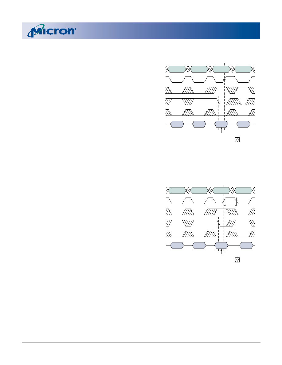
The configuration registers are loaded using a four-
step sequence consisting of two asynchronous READ
operations followed by two asynchronous WRITE
operations (see Figure 14). The read sequence is virtu-
ally identical except that an asynchronous READ is
performed during the fourth operation (see Figure 15).
Note that a third READ cycle of the highest address
cancels the access sequence until a different address is
read.
The address used during all READ and WRITE oper-
ations is the highest address of the CellularRAM device
being accessed (3FFFFFh for 64Mb, and 1FFFFFh for
32Mb); the content at this address is changed by using
this sequence (note that this is a deviation from the
CellularRAM specification).
The data value presented during the third operation
(WRITE) in the sequence defines whether the BCR or
the RCR is to be accessed. If the data is 0000h, the
sequence will access the RCR; if the data is 0001h, the
sequence will access the BCR. During the fourth oper-
ation, DQ[15:0] is used to transfer data into or out of
bits 15–0 of the configuration registers.
The use of the software sequence does not affect the
ability to perform the standard (CRE-controlled)
method of loading the configuration registers. How-
ever, the software nature of this access mechanism
eliminates the need for the control register enable
(CRE) ball. If the software mechanism is used, the CRE
ball can simply be tied to VSS. The port line often used
for CRE control purposes is no longer required.
Software access of the RCR should not be used to
enter or exit DPD.
Figure 14: Load Configuration Register
NOTE:
1. The WRITE on the third cycle must be CE#
controlled.
Figure 15: Read Configuration Register
NOTE:
1. The WRITE on the third cycle must be CE#
controlled.
2. CE# must be HIGH for 150ns before performing the
cycle that reads a configuration register.
ADDRESS
(MAX)
ADDRESS
(MAX)
ADDRESS
(MAX)
XXXXh
RCR: 0000h
BCR: 0001h
CR VALUE
IN
ADDRESS
CE#
OE#
WE#
LB#/UB#
DATA
DON'T CARE
READ
WRITE
1
WRITE
ADDRESS
(MAX)
ADDRESS
(MAX)
ADDRESS
(MAX)
ADDRESS
(MAX)
XXXXh
CR VALUE
OUT
ADDRESS
CE#
OE#
WE#
LB#/UB#
DATA
DON'T CARE
READ
WRITE
1
READ
RCR: 0000h
BCR: 0001h
NOTE
2
ADDRESS
(MAX)
相关PDF资料 |
PDF描述 |
|---|---|
| MT46H32M32LGCM-5IT:A | 32M X 32 DDR DRAM, 5 ns, PBGA90 |
| MT46HC32M16LFCX-75:B | 32M X 16 DDR DRAM, 7.5 ns, PBGA90 |
| MT46HC32M16LGCM-54IT:B | 32M X 16 DDR DRAM, 5.4 ns, PBGA90 |
| MT47H32M16BT-37VL:A | 32M X 16 DDR DRAM, 0.5 ns, PBGA92 |
| MT47H64M16HQ-3IT:G | 64M X 16 DDR DRAM, 0.4 ns, PBGA60 |
相关代理商/技术参数 |
参数描述 |
|---|---|
| MT45W2MW16BFB-601 WT | 制造商:Micron Technology Inc 功能描述: |
| MT45W2MW16BFB-701 WT | 制造商:Micron Technology Inc 功能描述: |
| MT45W2MW16BFB-706 WT | 制造商:Micron Technology Inc 功能描述:PSRAM ASYNC 1 32MBIT 2MX16 70NS 54VFBGA - Trays |
| MT45W2MW16BFB-708 WT | 制造商:Micron Technology Inc 功能描述:PSRAM ASYNC 1 32MBIT 2MX16 70NS - Trays |
| MT45W2MW16BFB-856 WT | 制造商:Micron Technology Inc 功能描述:PSRAM ASYNC 1 32MBIT 2MX16 85NS 54VFBGA - Trays |
发布紧急采购,3分钟左右您将得到回复。