- 您现在的位置:买卖IC网 > PDF目录180051 > M-ORSO82G51BM680-DB (LATTICE SEMICONDUCTOR CORP) FPGA, 1296 CLBS, 333000 GATES, PBGA680 PDF资料下载
参数资料
| 型号: | M-ORSO82G51BM680-DB |
| 厂商: | LATTICE SEMICONDUCTOR CORP |
| 元件分类: | FPGA |
| 英文描述: | FPGA, 1296 CLBS, 333000 GATES, PBGA680 |
| 封装: | PLASTIC, FBGA-680 |
| 文件页数: | 104/123页 |
| 文件大小: | 2207K |
| 代理商: | M-ORSO82G51BM680-DB |
第1页第2页第3页第4页第5页第6页第7页第8页第9页第10页第11页第12页第13页第14页第15页第16页第17页第18页第19页第20页第21页第22页第23页第24页第25页第26页第27页第28页第29页第30页第31页第32页第33页第34页第35页第36页第37页第38页第39页第40页第41页第42页第43页第44页第45页第46页第47页第48页第49页第50页第51页第52页第53页第54页第55页第56页第57页第58页第59页第60页第61页第62页第63页第64页第65页第66页第67页第68页第69页第70页第71页第72页第73页第74页第75页第76页第77页第78页第79页第80页第81页第82页第83页第84页第85页第86页第87页第88页第89页第90页第91页第92页第93页第94页第95页第96页第97页第98页第99页第100页第101页第102页第103页当前第104页第105页第106页第107页第108页第109页第110页第111页第112页第113页第114页第115页第116页第117页第118页第119页第120页第121页第122页第123页
Lattice Semiconductor
ORCA ORSO82G5 Data Sheet
81
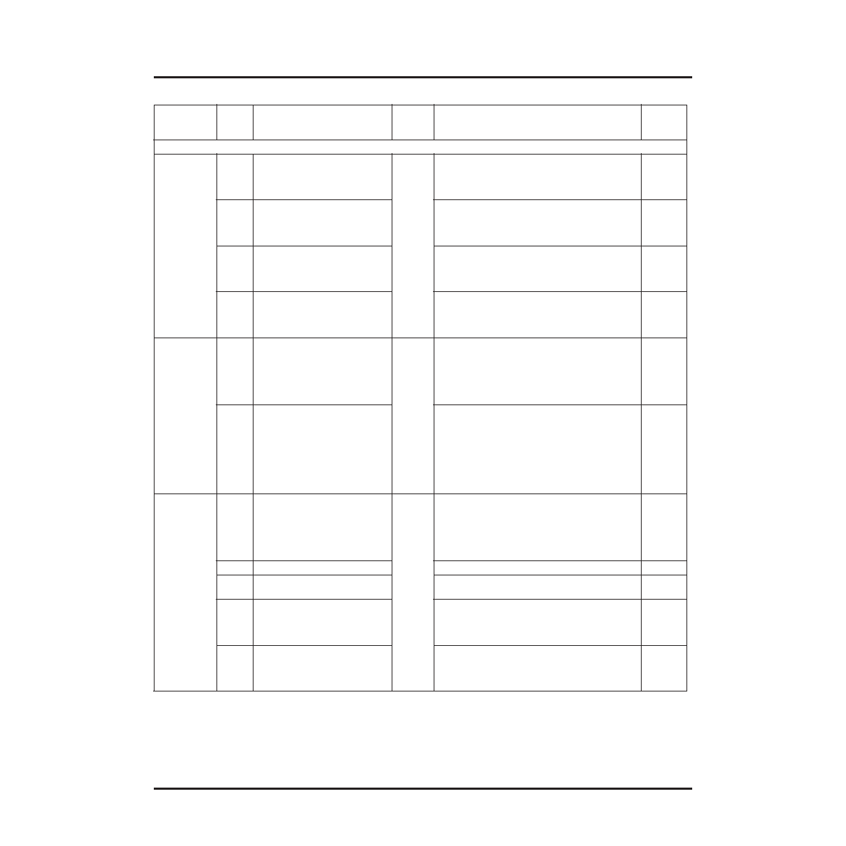
Table 21. Common Control Register Descriptions
(0x) Abso-
lute
Address
Bit
Name
Reset
Value
(0x)
Description
Mode
Common Control Registers (Read/Write)
30A00
[0:1]
RCKSELB
00
“00” - Channel BA source for clock RCK78B
“01” - Channel BB source for clock RCK78B
“10” - Channel BC source for clock RCK78B
“11” - Channel BD source for clock RCK78B
Both
[2:3]
TCKSELB
“00” - Channel BA source for clock TCK78B
“01” - Channel BB source for clock TCK78B
“10” - Channel BC source for clock TCK78B
“11” - Channel BD source for clock TCK78B
Both
[4:5]
RCKSELA
“00” - Channel AA source for clock RCK78A
“01” - Channel AB source for clock RCK78A
“10” - Channel AC source for clock RCK78A
“11” - Channel AD source for clock RCK78A
Both
[6:7]
TCKSELA
“00” - Channel AA source for clock TCK78A
“01” - Channel AB source for clock TCK78A
“10” - Channel AC source for clock TCK78A
“11” - Channel AD source for clock TCK78A
Both
30A01
[0:2]
CELL_SIZE
00
Cell Size, Three bits to set cell size.
“000” - Cell size is 76 bytes,
“001” - Cell size is 80 bytes,
“010” - Cell size is 84 bytes,
“011” - Cell size is 92 bytes
These are the only supported cell sizes.
Cell
[3:7]
RX_FIFO_MIN
Set Minimum threshold value for alignment
FIFO in SONET mode. When the read address
for the FIFO is below this value at the time
when write address is zero, it indicates that the
FIFO is near overow. This event will go high
only once during a frame when a framing byte
has been detected by the aligner. The default
threshold value is “00000”.
SONET
30A02
0
TX_DISABLE_ON_RDI
01
Transmitter Disable on RDI (Detection), If
TX_DISABLE_ON_RDI = 1 - No cell data is
transmitted on a link in which a RDI has been
detected by the corresponding link’s receiver. If
this bit is set to 0, cell data will be transmitted
on a link irrespective of detection of a RDI.
Cell
[1:3]
DEVICE_MODE
These bits should always be set to “001”
Cell
4
SCHAR_ENA
SCHAR_ENA = 1 enables SERDES character-
ization of SERDES B. Refer to section
Both
5
SCHAR_TXSEL
SCHAR_TXSEL =1 is a Select Tx option which
will cause chip ports to directly control the
SERDES low-speed transmit ports of one of
the channels selected by SCHAR_CHAN
Both
6:7
SCHAR_CHAN
“00” - Select channel BA to test
“01” - Select channel BB to test
“10” - Select channel BC to test
“11” - Select channel BD to test
Both
相关PDF资料 |
PDF描述 |
|---|---|
| M-ORSO82G52BM680-DB | FPGA, 1296 CLBS, 333000 GATES, PBGA680 |
| M-ORT82G51BM680-DB | FPGA, 1296 CLBS, 333000 GATES, PBGA680 |
| M-ORT82G52BM680-DB | FPGA, 1296 CLBS, 333000 GATES, PBGA680 |
| M.PI-1R1D12 | 1 ELEMENT, 1.1 uH, GENERAL PURPOSE INDUCTOR, SMD |
| M01-014-1452PA | 14 CONTACT(S), MALE, RIGHT ANGLE TELECOM AND DATACOM CONNECTOR, SOLDER |
相关代理商/技术参数 |
参数描述 |
|---|---|
| MORTAR-44LB | 制造商:3M Electronic Products Division 功能描述:3M(TM) FIRE BARRIER MORTAR, 44 98040056073 制造商:3M Electronic Products Division 功能描述:Fire Barrier 44 lb Bag |
| MO-RX3930 | 制造商:未知厂家 制造商全称:未知厂家 功能描述:FSK RECEIVER MODULE |
| MO-RX3930-FS | 制造商:未知厂家 制造商全称:未知厂家 功能描述:FSK RECEIVER MODULE |
| MO-RX3930-FS315M | 制造商:未知厂家 制造商全称:未知厂家 功能描述:FSK RECEIVER MODULE |
| MO-RX3930-FS434M | 制造商:未知厂家 制造商全称:未知厂家 功能描述:FSK RECEIVER MODULE |
发布紧急采购,3分钟左右您将得到回复。