- 您现在的位置:买卖IC网 > PDF目录180051 > M-ORSO82G51BM680-DB (LATTICE SEMICONDUCTOR CORP) FPGA, 1296 CLBS, 333000 GATES, PBGA680 PDF资料下载
参数资料
| 型号: | M-ORSO82G51BM680-DB |
| 厂商: | LATTICE SEMICONDUCTOR CORP |
| 元件分类: | FPGA |
| 英文描述: | FPGA, 1296 CLBS, 333000 GATES, PBGA680 |
| 封装: | PLASTIC, FBGA-680 |
| 文件页数: | 70/123页 |
| 文件大小: | 2207K |
| 代理商: | M-ORSO82G51BM680-DB |
第1页第2页第3页第4页第5页第6页第7页第8页第9页第10页第11页第12页第13页第14页第15页第16页第17页第18页第19页第20页第21页第22页第23页第24页第25页第26页第27页第28页第29页第30页第31页第32页第33页第34页第35页第36页第37页第38页第39页第40页第41页第42页第43页第44页第45页第46页第47页第48页第49页第50页第51页第52页第53页第54页第55页第56页第57页第58页第59页第60页第61页第62页第63页第64页第65页第66页第67页第68页第69页当前第70页第71页第72页第73页第74页第75页第76页第77页第78页第79页第80页第81页第82页第83页第84页第85页第86页第87页第88页第89页第90页第91页第92页第93页第94页第95页第96页第97页第98页第99页第100页第101页第102页第103页第104页第105页第106页第107页第108页第109页第110页第111页第112页第113页第114页第115页第116页第117页第118页第119页第120页第121页第122页第123页
Lattice Semiconductor
ORCA ORSO82G5 Data Sheet
50
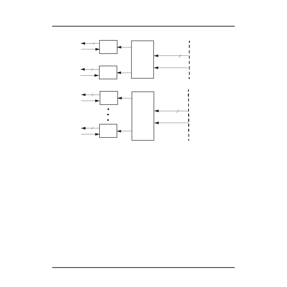
Figure 35. OPC2 and OPC8 Block Diagrams
TX FIFO Block
In cell mode, the TxFIFO block contains the write state machine and FIFO memory. The FIFO is used to retime the
cell data from the FPGA interface at a rate of 156 MHz to the framer rate of 77.76 MHz.
The FIFO memory is implemented as a 64 x 34 FIFO. The FIFO receives data as 33-bit words with the start-of-cell
as the MSB of each word. Thus each cell occupies a maximum size of 23 words. For each link, the memory must
be capable of holding at least 2 cells or 46 words (one for write and one for read). To ensure extra space, this
capacity has been increased to 64 words. In addition, an extra bit has been reserved to store the link idle cell indi-
cator bit which is used for indicating the internally generated idle cells. Thus each word in a cell is 34 bits. Data are
written to the memory on the 156 MHz clock domain and read on the 77.76 MHz clock domain by the
Tx_Frame_Processor block. The OPC requires no response from the TxFIFO for writing data. The TxFIFO is guar-
anteed by design to not overow or underrun.
TX Frame Processor
The Tx_Frame_Processor (TFP) block is the primary data processing block in the both SONET mode and cell
mode. It organizes the cell data into a SONET frame before sending it to the SERDES. In cell mode, the 32-bit data
comes from the TX FIFO block. The three major TFP sub-blocks were described in the SONET mode section.
In cell mode, the Payload sub block is activated by the link_frm_sync in cell mode. A pulse on this signal from the
OPC indicates the start of a frame. Each frame contains 4 different types of bytes in cell mode:
TOH bytes (Auto TOH mode only)
Link Header (LH) bytes
Cell payload bytes
Pad bytes
TX
FIFO
OPC2
Block
OPC2_[A:B][1:2][0:39]
SYSCLK156[A:B][1:2]
32
77.76 MHz
TX
FIFO
32
77.76 MHz
TX
FIFO
OPC8
OPC8[0:159]
SYSCLK156 8
32
77.76 MHz
TX
FIFO
32
77.76 MHz
LINK 0
LINK 1
LINK 0
LINK 7
40
160
FPGA
LOGIC
Block
FPGA
LOGIC
相关PDF资料 |
PDF描述 |
|---|---|
| M-ORSO82G52BM680-DB | FPGA, 1296 CLBS, 333000 GATES, PBGA680 |
| M-ORT82G51BM680-DB | FPGA, 1296 CLBS, 333000 GATES, PBGA680 |
| M-ORT82G52BM680-DB | FPGA, 1296 CLBS, 333000 GATES, PBGA680 |
| M.PI-1R1D12 | 1 ELEMENT, 1.1 uH, GENERAL PURPOSE INDUCTOR, SMD |
| M01-014-1452PA | 14 CONTACT(S), MALE, RIGHT ANGLE TELECOM AND DATACOM CONNECTOR, SOLDER |
相关代理商/技术参数 |
参数描述 |
|---|---|
| MORTAR-44LB | 制造商:3M Electronic Products Division 功能描述:3M(TM) FIRE BARRIER MORTAR, 44 98040056073 制造商:3M Electronic Products Division 功能描述:Fire Barrier 44 lb Bag |
| MO-RX3930 | 制造商:未知厂家 制造商全称:未知厂家 功能描述:FSK RECEIVER MODULE |
| MO-RX3930-FS | 制造商:未知厂家 制造商全称:未知厂家 功能描述:FSK RECEIVER MODULE |
| MO-RX3930-FS315M | 制造商:未知厂家 制造商全称:未知厂家 功能描述:FSK RECEIVER MODULE |
| MO-RX3930-FS434M | 制造商:未知厂家 制造商全称:未知厂家 功能描述:FSK RECEIVER MODULE |
发布紧急采购,3分钟左右您将得到回复。