- 您现在的位置:买卖IC网 > PDF目录180051 > M-ORSO82G51BM680-DB (LATTICE SEMICONDUCTOR CORP) FPGA, 1296 CLBS, 333000 GATES, PBGA680 PDF资料下载
参数资料
| 型号: | M-ORSO82G51BM680-DB |
| 厂商: | LATTICE SEMICONDUCTOR CORP |
| 元件分类: | FPGA |
| 英文描述: | FPGA, 1296 CLBS, 333000 GATES, PBGA680 |
| 封装: | PLASTIC, FBGA-680 |
| 文件页数: | 54/123页 |
| 文件大小: | 2207K |
| 代理商: | M-ORSO82G51BM680-DB |
第1页第2页第3页第4页第5页第6页第7页第8页第9页第10页第11页第12页第13页第14页第15页第16页第17页第18页第19页第20页第21页第22页第23页第24页第25页第26页第27页第28页第29页第30页第31页第32页第33页第34页第35页第36页第37页第38页第39页第40页第41页第42页第43页第44页第45页第46页第47页第48页第49页第50页第51页第52页第53页当前第54页第55页第56页第57页第58页第59页第60页第61页第62页第63页第64页第65页第66页第67页第68页第69页第70页第71页第72页第73页第74页第75页第76页第77页第78页第79页第80页第81页第82页第83页第84页第85页第86页第87页第88页第89页第90页第91页第92页第93页第94页第95页第96页第97页第98页第99页第100页第101页第102页第103页第104页第105页第106页第107页第108页第109页第110页第111页第112页第113页第114页第115页第116页第117页第118页第119页第120页第121页第122页第123页
Lattice Semiconductor
ORCA ORSO82G5 Data Sheet
36
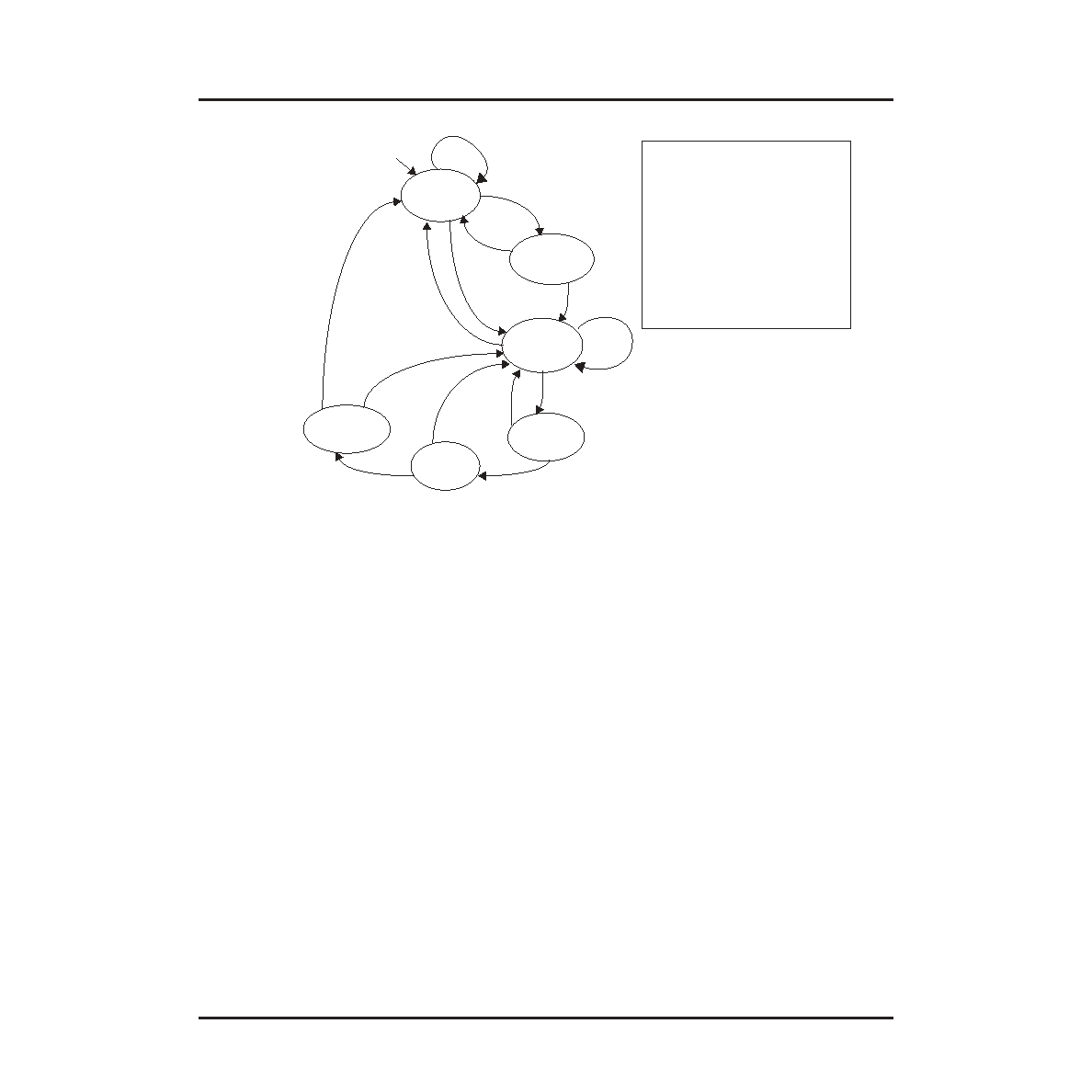
Figure 21. Framer State Machine
The framer FSM comes out of reset in the “OOF” state with the OOF alarm set. The framer goes in frame if it nds
2 consecutive frames with the desired framing bytes and goes out of frame if it nds 4 consecutive frames with at
least one framing bit error in each frame. Frame timing is also synchronized based on the STS-48 row and column
counters. This corresponds to SONET specication that it will take two consecutive valid framing patterns to frame
to an incoming signal. Outside the “OOF” state, the OOF alarm output is low.
Section (B1) BIP-8 Calculator
The section BIP-8 B1 byte in a given STS-N frame contains the scrambled BIP value for all scrambled bytes of the
previous frame. Except for the A1,A2 and J0 section overhead bytes, all bytes in a frame are scrambled. The Sec-
tion (B1) BIP-8 is calculated as the even parity of all bits in the current STS-48 frame. This value is compared to the
Section Overhead B1 byte of the next frame. A B1 parity error ag is also generated as a software alarm bit.
Descrambler
The data from the framer is descrambled using the SONET/SDH standard generator polynomial 1 + x
6 + x7. The
descrambling is performed in parallel on each 32-bit word per channel, synchronized to the frame pulse and can be
disabled through the software register bit.
RDI (Remote Defect Indicator) Monitor
The line RDI (RDI-L) is monitored through bits 2-0 of the K2 byte. Within the 32-bit descrambled data, a pattern of
“110” on bits 26-24 will indicate a RDI-L status. RDI-L must be detected in two consecutive frames before an rdi
alarm register bit is set. If fast_frame_mode is enabled, then the RDI alarm register bit will be set if RDI-L is
detected in one frame.
Receive FIFO
Clock domain transfers and multi-link de-skew are one of the most critical parts of this device. The main clock
domain transfer for the datapath is handled by the receive FIFO. For each link, there are two FIFOs. A 24 x 33 FIFO
is used in SONET mode.
The use of the FIFO is controlled by conguration bits.
Data can be sent from the descrambler directly to the FPGA bypassing the alignment FIFO. Data from each
pat_srch
reset
OOF=1
patdet & !ffm
new_frm
in_frm
patdet
OOF=0
!patdet
oof_one
oof_two
oof_three
Legend:
ffm ~ In fast frame mode
AND ffm
!ffm AND
patdet
!patdet
patdet
!patdet
patdet
!patdet
!ffm ~ In regular frame
mode
patdet ~ Correct 4A1/4A2
framing pattern
detected
!patdet ~ Correct 4A1/4A2
framing pattern
NOT detected
!patdet
patdet
相关PDF资料 |
PDF描述 |
|---|---|
| M-ORSO82G52BM680-DB | FPGA, 1296 CLBS, 333000 GATES, PBGA680 |
| M-ORT82G51BM680-DB | FPGA, 1296 CLBS, 333000 GATES, PBGA680 |
| M-ORT82G52BM680-DB | FPGA, 1296 CLBS, 333000 GATES, PBGA680 |
| M.PI-1R1D12 | 1 ELEMENT, 1.1 uH, GENERAL PURPOSE INDUCTOR, SMD |
| M01-014-1452PA | 14 CONTACT(S), MALE, RIGHT ANGLE TELECOM AND DATACOM CONNECTOR, SOLDER |
相关代理商/技术参数 |
参数描述 |
|---|---|
| MORTAR-44LB | 制造商:3M Electronic Products Division 功能描述:3M(TM) FIRE BARRIER MORTAR, 44 98040056073 制造商:3M Electronic Products Division 功能描述:Fire Barrier 44 lb Bag |
| MO-RX3930 | 制造商:未知厂家 制造商全称:未知厂家 功能描述:FSK RECEIVER MODULE |
| MO-RX3930-FS | 制造商:未知厂家 制造商全称:未知厂家 功能描述:FSK RECEIVER MODULE |
| MO-RX3930-FS315M | 制造商:未知厂家 制造商全称:未知厂家 功能描述:FSK RECEIVER MODULE |
| MO-RX3930-FS434M | 制造商:未知厂家 制造商全称:未知厂家 功能描述:FSK RECEIVER MODULE |
发布紧急采购,3分钟左右您将得到回复。