- 您现在的位置:买卖IC网 > PDF目录180051 > M-ORSO82G51BM680-DB (LATTICE SEMICONDUCTOR CORP) FPGA, 1296 CLBS, 333000 GATES, PBGA680 PDF资料下载
参数资料
| 型号: | M-ORSO82G51BM680-DB |
| 厂商: | LATTICE SEMICONDUCTOR CORP |
| 元件分类: | FPGA |
| 英文描述: | FPGA, 1296 CLBS, 333000 GATES, PBGA680 |
| 封装: | PLASTIC, FBGA-680 |
| 文件页数: | 67/123页 |
| 文件大小: | 2207K |
| 代理商: | M-ORSO82G51BM680-DB |
第1页第2页第3页第4页第5页第6页第7页第8页第9页第10页第11页第12页第13页第14页第15页第16页第17页第18页第19页第20页第21页第22页第23页第24页第25页第26页第27页第28页第29页第30页第31页第32页第33页第34页第35页第36页第37页第38页第39页第40页第41页第42页第43页第44页第45页第46页第47页第48页第49页第50页第51页第52页第53页第54页第55页第56页第57页第58页第59页第60页第61页第62页第63页第64页第65页第66页当前第67页第68页第69页第70页第71页第72页第73页第74页第75页第76页第77页第78页第79页第80页第81页第82页第83页第84页第85页第86页第87页第88页第89页第90页第91页第92页第93页第94页第95页第96页第97页第98页第99页第100页第101页第102页第103页第104页第105页第106页第107页第108页第109页第110页第111页第112页第113页第114页第115页第116页第117页第118页第119页第120页第121页第122页第123页
Lattice Semiconductor
ORCA ORSO82G5 Data Sheet
48
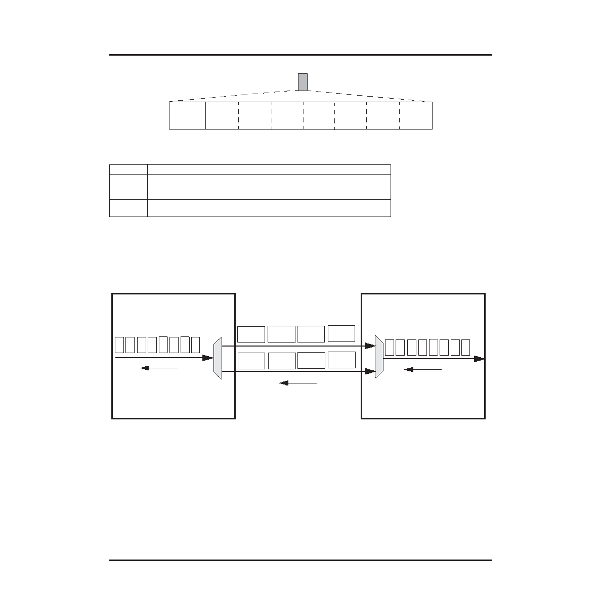
Figure 33. Link Header Byte
Table 8. Link Header Format
There is no way to tell where a cell starts unless one counts the cells from the beginning of the SPE. That means,
there is no way to regain lost cell delineation other than wait for the next SONET frame.
In Cell Mode, multiple SERDES links are used to achieve desired bandwidth. Data are cell-striped in a round-robin
fashion across two or eight links by the transmitter and then re-assembled back into a single cell stream (destrip-
ing) by the receiver. This is shown in Figure 34.
Figure 34. Multi-Link Interface - Two-Link Example
To assist with cell delineation, each link transmitter assigns sequence numbers to cells (LSEQN[6:0] bits in the Link
Header byte) before sending them out on the link. Each link increments its sequence numbers independently as
shown in Figure 34. All links reset their sequence number generator at the beginning of a SONET frame (All links
are synchronized to the start of a frame).
On the receiving side, each receiver uses the sequence numbers to verify the correct cell delineation. Since the
links were synchronized to the start of the SONET frame, all links will have cells with the same sequence number
available at the same time (although deskew needs to happen to properly align the cells). This allows the receiver
to correctly reconstruct the original cell stream.
If an unexpected sequence number is received, the receiver does not use the received value as the basis for the
next expected sequence number. Rather the old expected value is incremented by one, forming the new expected
value. An error ag is sent to the software register interface and the cell will be marked with an error. For example,
assume that the receiver expected to receive a cell with sequence number 27, but received one with sequence
Location
Field/Description
7
Idle - Idle Cell Indicator
0: User Cell (contains valid data)
1: Idle Cell (no data in the cell payload)
6:0
LSEQ - Link Sequence Number. This value is used when aligning cells from
multiple links when doing link group multiplexing.
LIDLE
LSEQN[6:0]
LINK HEADER BYTE
Time
TRANSMITTER
Time
3
2
1
0
7
6
5
4
CELL STRIPING
0
1
LSEQ = 3
Cell = 7
LSEQ = 2
Cell = 5
LSEQ = 1
Cell = 3
LSEQ = 0
Cell = 1
Time
RECEIVER
3
2
1
0
7
6
5
4
CELL DE-STRIPING
0
1
LSEQ = 3
Cell = 6
LSEQ = 2
Cell = 4
LSEQ = 1
Cell = 2
LSEQ = 0
Cell = 0
相关PDF资料 |
PDF描述 |
|---|---|
| M-ORSO82G52BM680-DB | FPGA, 1296 CLBS, 333000 GATES, PBGA680 |
| M-ORT82G51BM680-DB | FPGA, 1296 CLBS, 333000 GATES, PBGA680 |
| M-ORT82G52BM680-DB | FPGA, 1296 CLBS, 333000 GATES, PBGA680 |
| M.PI-1R1D12 | 1 ELEMENT, 1.1 uH, GENERAL PURPOSE INDUCTOR, SMD |
| M01-014-1452PA | 14 CONTACT(S), MALE, RIGHT ANGLE TELECOM AND DATACOM CONNECTOR, SOLDER |
相关代理商/技术参数 |
参数描述 |
|---|---|
| MORTAR-44LB | 制造商:3M Electronic Products Division 功能描述:3M(TM) FIRE BARRIER MORTAR, 44 98040056073 制造商:3M Electronic Products Division 功能描述:Fire Barrier 44 lb Bag |
| MO-RX3930 | 制造商:未知厂家 制造商全称:未知厂家 功能描述:FSK RECEIVER MODULE |
| MO-RX3930-FS | 制造商:未知厂家 制造商全称:未知厂家 功能描述:FSK RECEIVER MODULE |
| MO-RX3930-FS315M | 制造商:未知厂家 制造商全称:未知厂家 功能描述:FSK RECEIVER MODULE |
| MO-RX3930-FS434M | 制造商:未知厂家 制造商全称:未知厂家 功能描述:FSK RECEIVER MODULE |
发布紧急采购,3分钟左右您将得到回复。