- 您现在的位置:买卖IC网 > PDF目录180051 > M-ORSO82G51BM680-DB (LATTICE SEMICONDUCTOR CORP) FPGA, 1296 CLBS, 333000 GATES, PBGA680 PDF资料下载
参数资料
| 型号: | M-ORSO82G51BM680-DB |
| 厂商: | LATTICE SEMICONDUCTOR CORP |
| 元件分类: | FPGA |
| 英文描述: | FPGA, 1296 CLBS, 333000 GATES, PBGA680 |
| 封装: | PLASTIC, FBGA-680 |
| 文件页数: | 31/123页 |
| 文件大小: | 2207K |
| 代理商: | M-ORSO82G51BM680-DB |
第1页第2页第3页第4页第5页第6页第7页第8页第9页第10页第11页第12页第13页第14页第15页第16页第17页第18页第19页第20页第21页第22页第23页第24页第25页第26页第27页第28页第29页第30页当前第31页第32页第33页第34页第35页第36页第37页第38页第39页第40页第41页第42页第43页第44页第45页第46页第47页第48页第49页第50页第51页第52页第53页第54页第55页第56页第57页第58页第59页第60页第61页第62页第63页第64页第65页第66页第67页第68页第69页第70页第71页第72页第73页第74页第75页第76页第77页第78页第79页第80页第81页第82页第83页第84页第85页第86页第87页第88页第89页第90页第91页第92页第93页第94页第95页第96页第97页第98页第99页第100页第101页第102页第103页第104页第105页第106页第107页第108页第109页第110页第111页第112页第113页第114页第115页第116页第117页第118页第119页第120页第121页第122页第123页
Lattice Semiconductor
ORCA ORSO82G5 Data Sheet
15
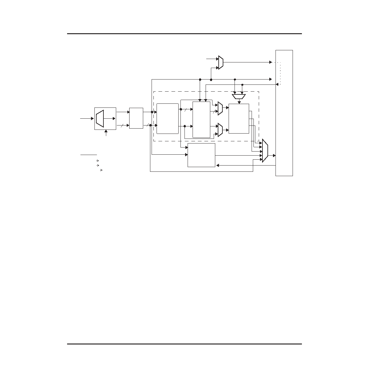
Figure 4. Top Level Overview, RX Path Logic, Single Channel
SERializer and DESerializer (SERDES)
Each SERDES block is a quad transceiver containing 4 channels for serial data transmission, with a per-channel
selectable data rate of 1.0—2.7 Gbits/s. Each SERDES block features high-speed CML interfaces and is designed
to operate in SONET backplane applications. The transceiver is controlled and congured via an 8-bit, 16-bit or 32-
bit MicroProcessor Interface through the FPGA. Each channel has dedicated registers that are readable and writ-
able. The device also contains global registers for control of common circuitry and functions. There are two SER-
DES blocks (or two quads), A and B, in the embedded portion of the device. Each quad supports four full duplex
serial links (Slice A contains channels AA, AB, AC, and AD while slice B contains channels BA, BB, BC, and BD).
Each SERDES block contains its own dedicated PLLs for transmit and receive clock generation. The user provides
a reference clock of the appropriate frequency (one per SERDES quad). The receiver PLLs extract the clock from
the serial input data and retime the data with the recovered clock. Clock divider circuitry also provides reference
clocks for the FPGA logic.
8:32 MUX and 32:8 DEMUX
The purpose of the MUX/DEMUX block is to provide a wide, low-speed interface at the FPGA portion of the
ORSO82G5 for each channel or data lane. The interface to the SERDES macro runs at 1/8th the bit rate of the data
lane. The MUX/DEMUX converts the data rate and bit-width so the FPGA core can run at 1/4th this frequency (i.e.,
1/32nd the SERDES rate). This gives a range of 31.25 MHz—84.38 MHz for the data crossing the FPGA/embed-
ded core boundary on SERDES only and SONET modes.
SONET Transmit OverHead (TOH) Processing, Framer and Scrambler/Descrambler (SONET and Cell
Modes)
In the transmit direction, the TOH block is responsible for processing the 144 (48 x 3) TOH bytes at the beginning of
each row of the transport frame. The TOH bytes may be transmitted transparently from the FPGA logic or may be
inserted by the TOH block (AUTO_TOH mode).
FPGA
Logic
Embedded Core
8:32
demux
Channel
Align,
(24x33)
FIFO
SONET
Framer
Decrambler
FPGA Data
SONET Processing
1.0-2.7Gbps
SERDES
8
LDOUT
RBC
1:8
dem
ux
8b
REFCLK
(155.52MHZ)
LEGEND:
RCK78x
x = A for Quad A, B for Quad B
RWCKxx
xx = [AA, AD] or [BA,BD]
IPCj_DOUT
j = [1,2]
SPE
Generator
Cell extractor,
RDXFIFO, IPC
SPE
DOUTxx_FP
DOUTxx[31:0]
32
FP
IPCj_DOUT
SYSCLK156x[1,2]
32
FP
From Other 3 Links
in Quad
77.76MHZ
RCK78x
RWCKxx
RSYSCLKx[1,2]
相关PDF资料 |
PDF描述 |
|---|---|
| M-ORSO82G52BM680-DB | FPGA, 1296 CLBS, 333000 GATES, PBGA680 |
| M-ORT82G51BM680-DB | FPGA, 1296 CLBS, 333000 GATES, PBGA680 |
| M-ORT82G52BM680-DB | FPGA, 1296 CLBS, 333000 GATES, PBGA680 |
| M.PI-1R1D12 | 1 ELEMENT, 1.1 uH, GENERAL PURPOSE INDUCTOR, SMD |
| M01-014-1452PA | 14 CONTACT(S), MALE, RIGHT ANGLE TELECOM AND DATACOM CONNECTOR, SOLDER |
相关代理商/技术参数 |
参数描述 |
|---|---|
| MORTAR-44LB | 制造商:3M Electronic Products Division 功能描述:3M(TM) FIRE BARRIER MORTAR, 44 98040056073 制造商:3M Electronic Products Division 功能描述:Fire Barrier 44 lb Bag |
| MO-RX3930 | 制造商:未知厂家 制造商全称:未知厂家 功能描述:FSK RECEIVER MODULE |
| MO-RX3930-FS | 制造商:未知厂家 制造商全称:未知厂家 功能描述:FSK RECEIVER MODULE |
| MO-RX3930-FS315M | 制造商:未知厂家 制造商全称:未知厂家 功能描述:FSK RECEIVER MODULE |
| MO-RX3930-FS434M | 制造商:未知厂家 制造商全称:未知厂家 功能描述:FSK RECEIVER MODULE |
发布紧急采购,3分钟左右您将得到回复。