- 您现在的位置:买卖IC网 > PDF目录180051 > M-ORSO82G51BM680-DB (LATTICE SEMICONDUCTOR CORP) FPGA, 1296 CLBS, 333000 GATES, PBGA680 PDF资料下载
参数资料
| 型号: | M-ORSO82G51BM680-DB |
| 厂商: | LATTICE SEMICONDUCTOR CORP |
| 元件分类: | FPGA |
| 英文描述: | FPGA, 1296 CLBS, 333000 GATES, PBGA680 |
| 封装: | PLASTIC, FBGA-680 |
| 文件页数: | 71/123页 |
| 文件大小: | 2207K |
| 代理商: | M-ORSO82G51BM680-DB |
第1页第2页第3页第4页第5页第6页第7页第8页第9页第10页第11页第12页第13页第14页第15页第16页第17页第18页第19页第20页第21页第22页第23页第24页第25页第26页第27页第28页第29页第30页第31页第32页第33页第34页第35页第36页第37页第38页第39页第40页第41页第42页第43页第44页第45页第46页第47页第48页第49页第50页第51页第52页第53页第54页第55页第56页第57页第58页第59页第60页第61页第62页第63页第64页第65页第66页第67页第68页第69页第70页当前第71页第72页第73页第74页第75页第76页第77页第78页第79页第80页第81页第82页第83页第84页第85页第86页第87页第88页第89页第90页第91页第92页第93页第94页第95页第96页第97页第98页第99页第100页第101页第102页第103页第104页第105页第106页第107页第108页第109页第110页第111页第112页第113页第114页第115页第116页第117页第118页第119页第120页第121页第122页第123页
Lattice Semiconductor
ORCA ORSO82G5 Data Sheet
51
There are N x 3 (N = 48) bytes of TOH per row and there are a total of 9 rows in a SONET frame. In cell mode, the
rest of the bytes in each row after the TOH bytes are lled by cells. The rst byte in a cell is a Link Header (LH) byte.
At the end of each frame, there are pad bytes if required.
An important function of the payload block is the grouping of bytes together to be presented to the scramble logic.
Due to the insertion of the LH byte in each cell, the total cell data are not divisible by 4 (4 bytes are sent per 77.76
MHz clock cycle). At the end of each row within a SONET frame, the payload block stops sending cell data and
indicates to the TOH block to insert the next row’s TOH bytes. At the end of the TOH byte transmission, the cell data
transmission is resumed.
At the end of a cell, the cell’s BIP-8 byte is inserted. The next cell’s Link Header byte (LH) immediately follows the
previous cell’s BIP-8 byte. The MSB of the LH byte is the link idle cell indicator bit. The payload block gets this bit
from the MSB of the rst word of a cell in the memory and inserts it into the LH byte for the appropriate cell. The
rest of the LH byte is the link sequence number. This number is incremented for each subsequent cell.
After all cells have been transmitted, the appropriate number of pad bytes are sent. At a link speed of 2.5 GHz,
there are 38,880 bytes (SPE + TOH) per frame. There are 1296 bytes of TOH and 37,584 bytes of SPE. For cell
data of 85 bytes this translates to 442 cells per frame and 14 pad bytes (# of cells per frame = # of bytes of SPE/#
of bytes in a cell).
Cell Mode Transmit Timing
Figure 36 shows the transmit clocks and recommended clocking scheme in cell mode. TCK156A, TCK151B can be
used as a 156 MHz clock source for SYSCLK156[A1, A2] and SYSCLK156[B1, B2] respectively. SYSCLK156[A1,
A2] and SYSCLK[B1, B2] are shared with the receive logic in cell mode.
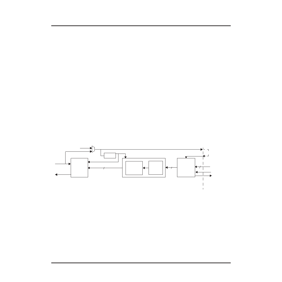
Figure 36. Cell Mode Transmit Timing
When operating in the two-link CELL MODE, each OPC2 Block passes User cells from FPGA to embedded core.
Depending upon the congured CELL SIZE, cell transfers will take a variable number of SYSCLK156 cycles to be
transmitted across the interface. Data are always transferred across a 40-bit bus (5 octets per clock cycle).
Figure 37 shows 16 clock cycles for a cell transfer this corresponds to a User Cell size of 79 octets. The two control
signals in the gure are dened as:
cell_begin_ok: cell request signal from core to FPGA. It will be asserted every 20 or 16 clock cycles (depending
on cell size) when the core is ready to accept cells from FPGA.
If core FIFO cannot accept cells, cell_begin_ok will be low.
If core FIFO is empty then cell_begin_ok will be asserted every 4 clock cycles until cellvalid is asserted by user
to indicate valid cell data.
cellvalid: Clock-wide pulse asserted by user to indicate valid data. Asserted on the clock cycle following
cell_begin_ok.
OPC
xck311
LDIN[7:0]
311.04 MHz
32:8 MUX
TFP
TxFIFO
32
161 bits
FPGA
Cell Data
FROM OTHER LINKS
TCK78A
SYSCLK156[A1, A2]
]
Cell Valid
Backpressure
Signal
1/2
TCK156A (XCK/2)
or SYSCLK568
相关PDF资料 |
PDF描述 |
|---|---|
| M-ORSO82G52BM680-DB | FPGA, 1296 CLBS, 333000 GATES, PBGA680 |
| M-ORT82G51BM680-DB | FPGA, 1296 CLBS, 333000 GATES, PBGA680 |
| M-ORT82G52BM680-DB | FPGA, 1296 CLBS, 333000 GATES, PBGA680 |
| M.PI-1R1D12 | 1 ELEMENT, 1.1 uH, GENERAL PURPOSE INDUCTOR, SMD |
| M01-014-1452PA | 14 CONTACT(S), MALE, RIGHT ANGLE TELECOM AND DATACOM CONNECTOR, SOLDER |
相关代理商/技术参数 |
参数描述 |
|---|---|
| MORTAR-44LB | 制造商:3M Electronic Products Division 功能描述:3M(TM) FIRE BARRIER MORTAR, 44 98040056073 制造商:3M Electronic Products Division 功能描述:Fire Barrier 44 lb Bag |
| MO-RX3930 | 制造商:未知厂家 制造商全称:未知厂家 功能描述:FSK RECEIVER MODULE |
| MO-RX3930-FS | 制造商:未知厂家 制造商全称:未知厂家 功能描述:FSK RECEIVER MODULE |
| MO-RX3930-FS315M | 制造商:未知厂家 制造商全称:未知厂家 功能描述:FSK RECEIVER MODULE |
| MO-RX3930-FS434M | 制造商:未知厂家 制造商全称:未知厂家 功能描述:FSK RECEIVER MODULE |
发布紧急采购,3分钟左右您将得到回复。