- 您现在的位置:买卖IC网 > PDF目录180051 > M-ORSO82G51BM680-DB (LATTICE SEMICONDUCTOR CORP) FPGA, 1296 CLBS, 333000 GATES, PBGA680 PDF资料下载
参数资料
| 型号: | M-ORSO82G51BM680-DB |
| 厂商: | LATTICE SEMICONDUCTOR CORP |
| 元件分类: | FPGA |
| 英文描述: | FPGA, 1296 CLBS, 333000 GATES, PBGA680 |
| 封装: | PLASTIC, FBGA-680 |
| 文件页数: | 3/123页 |
| 文件大小: | 2207K |
| 代理商: | M-ORSO82G51BM680-DB |
第1页第2页当前第3页第4页第5页第6页第7页第8页第9页第10页第11页第12页第13页第14页第15页第16页第17页第18页第19页第20页第21页第22页第23页第24页第25页第26页第27页第28页第29页第30页第31页第32页第33页第34页第35页第36页第37页第38页第39页第40页第41页第42页第43页第44页第45页第46页第47页第48页第49页第50页第51页第52页第53页第54页第55页第56页第57页第58页第59页第60页第61页第62页第63页第64页第65页第66页第67页第68页第69页第70页第71页第72页第73页第74页第75页第76页第77页第78页第79页第80页第81页第82页第83页第84页第85页第86页第87页第88页第89页第90页第91页第92页第93页第94页第95页第96页第97页第98页第99页第100页第101页第102页第103页第104页第105页第106页第107页第108页第109页第110页第111页第112页第113页第114页第115页第116页第117页第118页第119页第120页第121页第122页第123页
Lattice Semiconductor
ORCA ORSO82G5 Data Sheet
100
Package Pinouts
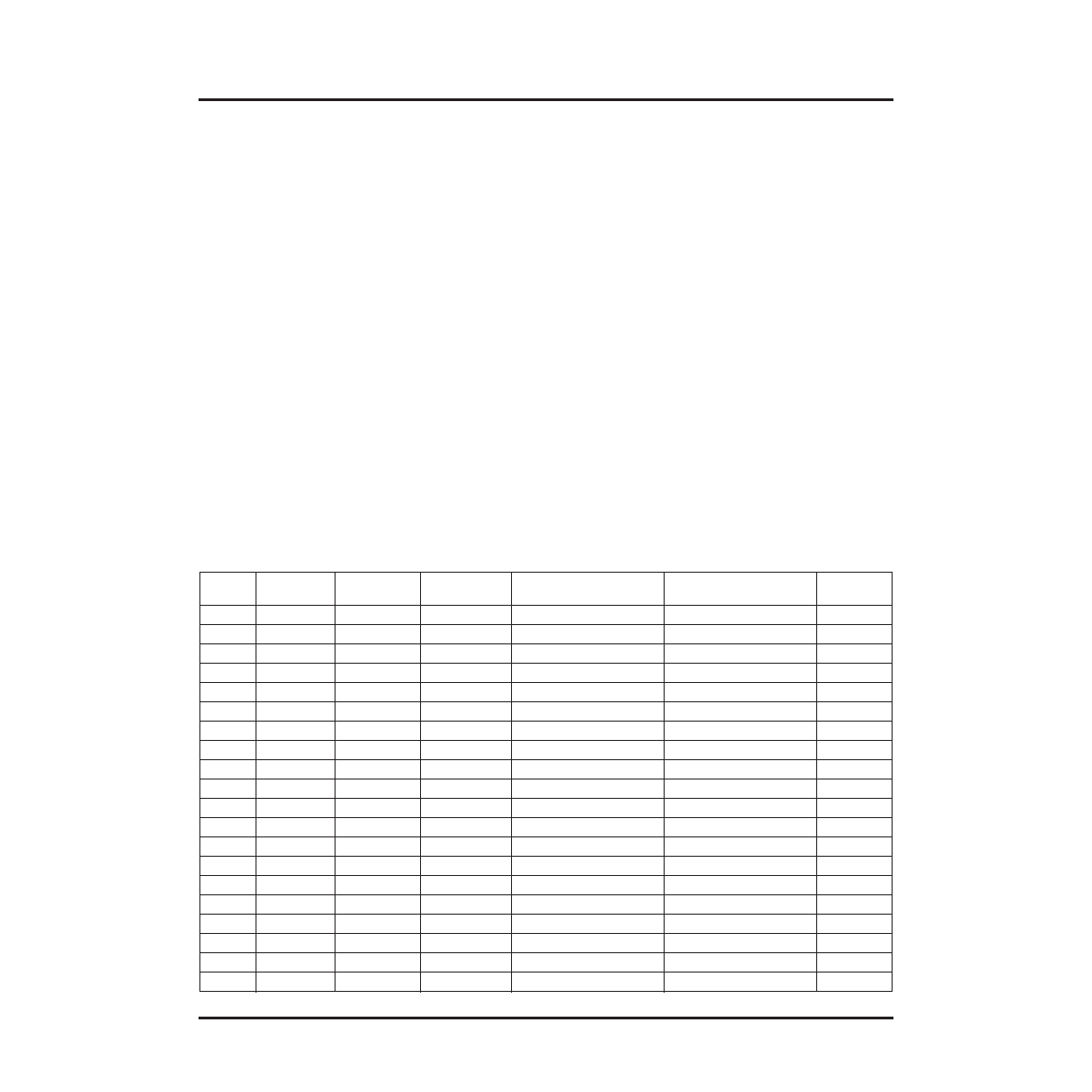
Table 35 provides the package pin and pin function for the ORSO82G5 FPSC and packages. The bond pad name
is identied in the PIO nomenclature used in the ispLEVER development system design editor. The Bank column
provides information as to which output voltage level bank the given pin is in. The Group column provides informa-
tion as to the group of pins the given pin is in. This is used to show which VREF pin is used to provide the reference
voltage for single-ended limited-swing I/Os. If none of these buffer types (such as SSTL, GTL, HSTL) are used in a
given group, then the VREF pin is available as an I/O pin.
When the number of FPGA bond pads exceeds the number of package pins, bond pads are unused. When the
number of package pins exceeds the number of bond pads, package pins are left unconnected (no connects).
When a package pin is to be left as a no connect for a specic die, it is indicated as a note in the device column for
the FPGA. The tables provide no information on unused pads.
As shown in the pair columns in Table 35, differential pairs and physical locations are numbered within each bank
(e.g., L19C-A0 is the nineteenth pair in an associated bank). A “C” indicates complementary differential, whereas a
“T” indicates true differential. An _A0 indicates the physical location of adjacent balls in either the horizontal or ver-
tical direction. Other physical indicators are as follows:
_A1 indicates one ball between pairs.
_A2 indicates two balls between pairs.
_D0 indicates balls are diagonally adjacent.
_D1 indicates balls are diagonally adjacent, separated by one physical ball.
VREF pins, shown in the Pin Description column in Table 35, are associated to the bank and group (e.g.,
VREF_TL_01 is the VREF for group one of the Top Left (TL) bank).
Table 35. ORSO82G5 680-Pin PBGAM Pinou
BM680
VDDIO
Bank
VREF
Group
I/O
Pin Description
Additional Function
BM680
Pair
AB20
—
Vss
—
C3
—
VDD33
—
E4
—
O
PRD_DATA
RD_DATA/TDO
—
F5
—
I
PRESET_N
RESET_N
—
G5
—
I
PRD_CFG_N
RD_CFG_N
—
D3
—
I
PPRGRM_N
PRGRM_N
—
A2
0 (TL)
—
VDDIO0
—
F4
0 (TL)
7
IO
PL2D
PLL_CK0C/HPPLL
L21C_A0
G4
0 (TL)
7
IO
PL2C
PLL_CK0T/HPPLL
L21T_A0
B3
0 (TL)
—
VDDIO0
—
C2
0 (TL)
7
IO
PL3D
—
L22C_D0
B1
0 (TL)
7
IO
PL3C
VREF_0_07
L22T_D0
A1
—
Vss
VSS
—
J5
0 (TL)
7
IO
PL4D
D5
L23C_A0
H5
0 (TL)
7
IO
PL4C
D6
L23T_A0
B7
0 (TL)
—
VDDIO0
—
E3
0 (TL)
8
IO
PL4B
—
L24C_A0
F3
0 (TL)
8
IO
PL4A
VREF_0_08
L24T_A0
C1
0 (TL)
8
IO
PL5D
HDC
L25C_D0
D2
0 (TL)
8
IO
PL5C
LDC_N
L25T_D0
相关PDF资料 |
PDF描述 |
|---|---|
| M-ORSO82G52BM680-DB | FPGA, 1296 CLBS, 333000 GATES, PBGA680 |
| M-ORT82G51BM680-DB | FPGA, 1296 CLBS, 333000 GATES, PBGA680 |
| M-ORT82G52BM680-DB | FPGA, 1296 CLBS, 333000 GATES, PBGA680 |
| M.PI-1R1D12 | 1 ELEMENT, 1.1 uH, GENERAL PURPOSE INDUCTOR, SMD |
| M01-014-1452PA | 14 CONTACT(S), MALE, RIGHT ANGLE TELECOM AND DATACOM CONNECTOR, SOLDER |
相关代理商/技术参数 |
参数描述 |
|---|---|
| MORTAR-44LB | 制造商:3M Electronic Products Division 功能描述:3M(TM) FIRE BARRIER MORTAR, 44 98040056073 制造商:3M Electronic Products Division 功能描述:Fire Barrier 44 lb Bag |
| MO-RX3930 | 制造商:未知厂家 制造商全称:未知厂家 功能描述:FSK RECEIVER MODULE |
| MO-RX3930-FS | 制造商:未知厂家 制造商全称:未知厂家 功能描述:FSK RECEIVER MODULE |
| MO-RX3930-FS315M | 制造商:未知厂家 制造商全称:未知厂家 功能描述:FSK RECEIVER MODULE |
| MO-RX3930-FS434M | 制造商:未知厂家 制造商全称:未知厂家 功能描述:FSK RECEIVER MODULE |
发布紧急采购,3分钟左右您将得到回复。