- 您现在的位置:买卖IC网 > PDF目录180051 > M-ORSO82G51BM680-DB (LATTICE SEMICONDUCTOR CORP) FPGA, 1296 CLBS, 333000 GATES, PBGA680 PDF资料下载
参数资料
| 型号: | M-ORSO82G51BM680-DB |
| 厂商: | LATTICE SEMICONDUCTOR CORP |
| 元件分类: | FPGA |
| 英文描述: | FPGA, 1296 CLBS, 333000 GATES, PBGA680 |
| 封装: | PLASTIC, FBGA-680 |
| 文件页数: | 65/123页 |
| 文件大小: | 2207K |
| 代理商: | M-ORSO82G51BM680-DB |
第1页第2页第3页第4页第5页第6页第7页第8页第9页第10页第11页第12页第13页第14页第15页第16页第17页第18页第19页第20页第21页第22页第23页第24页第25页第26页第27页第28页第29页第30页第31页第32页第33页第34页第35页第36页第37页第38页第39页第40页第41页第42页第43页第44页第45页第46页第47页第48页第49页第50页第51页第52页第53页第54页第55页第56页第57页第58页第59页第60页第61页第62页第63页第64页当前第65页第66页第67页第68页第69页第70页第71页第72页第73页第74页第75页第76页第77页第78页第79页第80页第81页第82页第83页第84页第85页第86页第87页第88页第89页第90页第91页第92页第93页第94页第95页第96页第97页第98页第99页第100页第101页第102页第103页第104页第105页第106页第107页第108页第109页第110页第111页第112页第113页第114页第115页第116页第117页第118页第119页第120页第121页第122页第123页
Lattice Semiconductor
ORCA ORSO82G5 Data Sheet
46
Cell Mode Detailed Description
A common application for the ORSO82G5 is to provide a bridge between a port card and a cell-based switch fabric.
In cell mode, the data in the Synchronous Payload Envelope (SPE) of the SONET frames is further formatted into
xed-length cells by the ORSO82G5. The cell contents will typically be unique to specic port card and switch
devices. The ORSO82G5 supports this application with a "cell mode" of operation
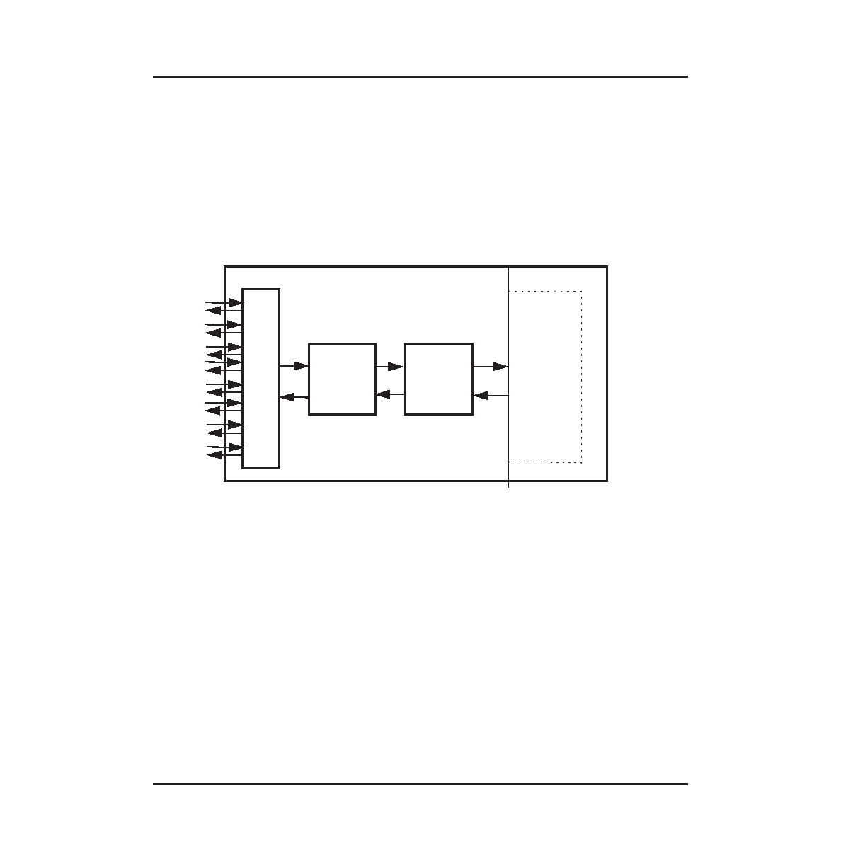
The basic data ows in cell mode are shown in Table 31. Data to be transmitted is received from the FPGA logic
(see Table 9 for details of the core/FPGA signal assignments which differ signicantly from the SERDES only and
SONET modes), inserted into the SPE of the SONET frame, scrambled and transmitted from the SERDES block.
In cell mode, multiple SERDES links are used to achieve desired bandwidth. Both two-link and eight-link cell
modes are supported. For such interfaces, data are cell-striped in a round-robin fashion across multiple links by the
transmitter.
Figure 31. Basic Data Flows - Cell Mode
In the receive direction, the framed data are received from the SERDES block, descrambled and are passed into a
cell extractor which extracts individual cells from the payload portion of the SONET frame. The cells are then
passed through a FIFO that performs lane-to-lane deskew and a clock domain transfer. The clock domain transfer
is handled automatically using idle cell insertion and deletion.
The cells are passed into either the eight-link Input Port Controller IPC8 block or to one of the four two-link
IPC2_[A:B][1:2] block(s) which reassemble the cells back into a single cell stream (destriping) which is sent to the
FPGA logic. (See Table 10 for details of the core/FPGA signal assignments. As with the transmit path, the cell
mode assignments differ signicantly from those for the SERDES only and SONET modes).
SERDES and SONET processing has been described in previous sections and only features unique to the cell
mode will be discussed in the following sections. The cell format will be discussed rst, followed by a description of
the transmit path, which will include either a two-link or an eight-link Output Port Controller (OPC) block, and a
description of the receive path, including the two-link or eight-link Input Port Controller (IPC) blocks.
Cell Formats
Cells are arranged within a SONET (STS-48c) frame as shown in Figure 32. A SONET STS-48c frame has 4176
(87 x 48) columns of SPE and 9 rows that gives a total of 37,584 bytes. In this implementation, data in a SPE is lim-
ited to xed size cells. Though four cell sizes are supported, only one cell size can be used at a time.
Receive (RX) Path
Transmit (TX) Path
Cell
Processing
Pseudo-
SONET
Processing
MUX/DEMUX
&
SERDES
ORCA 4E04
FPGA
Logic
Configurable
as
8
data
channels
Organized
in
two
four
channel
blocks
(quads)
User
Configurab
le
I/O
相关PDF资料 |
PDF描述 |
|---|---|
| M-ORSO82G52BM680-DB | FPGA, 1296 CLBS, 333000 GATES, PBGA680 |
| M-ORT82G51BM680-DB | FPGA, 1296 CLBS, 333000 GATES, PBGA680 |
| M-ORT82G52BM680-DB | FPGA, 1296 CLBS, 333000 GATES, PBGA680 |
| M.PI-1R1D12 | 1 ELEMENT, 1.1 uH, GENERAL PURPOSE INDUCTOR, SMD |
| M01-014-1452PA | 14 CONTACT(S), MALE, RIGHT ANGLE TELECOM AND DATACOM CONNECTOR, SOLDER |
相关代理商/技术参数 |
参数描述 |
|---|---|
| MORTAR-44LB | 制造商:3M Electronic Products Division 功能描述:3M(TM) FIRE BARRIER MORTAR, 44 98040056073 制造商:3M Electronic Products Division 功能描述:Fire Barrier 44 lb Bag |
| MO-RX3930 | 制造商:未知厂家 制造商全称:未知厂家 功能描述:FSK RECEIVER MODULE |
| MO-RX3930-FS | 制造商:未知厂家 制造商全称:未知厂家 功能描述:FSK RECEIVER MODULE |
| MO-RX3930-FS315M | 制造商:未知厂家 制造商全称:未知厂家 功能描述:FSK RECEIVER MODULE |
| MO-RX3930-FS434M | 制造商:未知厂家 制造商全称:未知厂家 功能描述:FSK RECEIVER MODULE |
发布紧急采购,3分钟左右您将得到回复。