- 您现在的位置:买卖IC网 > PDF目录180051 > M-ORSO82G51BM680-DB (LATTICE SEMICONDUCTOR CORP) FPGA, 1296 CLBS, 333000 GATES, PBGA680 PDF资料下载
参数资料
| 型号: | M-ORSO82G51BM680-DB |
| 厂商: | LATTICE SEMICONDUCTOR CORP |
| 元件分类: | FPGA |
| 英文描述: | FPGA, 1296 CLBS, 333000 GATES, PBGA680 |
| 封装: | PLASTIC, FBGA-680 |
| 文件页数: | 111/123页 |
| 文件大小: | 2207K |
| 代理商: | M-ORSO82G51BM680-DB |
第1页第2页第3页第4页第5页第6页第7页第8页第9页第10页第11页第12页第13页第14页第15页第16页第17页第18页第19页第20页第21页第22页第23页第24页第25页第26页第27页第28页第29页第30页第31页第32页第33页第34页第35页第36页第37页第38页第39页第40页第41页第42页第43页第44页第45页第46页第47页第48页第49页第50页第51页第52页第53页第54页第55页第56页第57页第58页第59页第60页第61页第62页第63页第64页第65页第66页第67页第68页第69页第70页第71页第72页第73页第74页第75页第76页第77页第78页第79页第80页第81页第82页第83页第84页第85页第86页第87页第88页第89页第90页第91页第92页第93页第94页第95页第96页第97页第98页第99页第100页第101页第102页第103页第104页第105页第106页第107页第108页第109页第110页当前第111页第112页第113页第114页第115页第116页第117页第118页第119页第120页第121页第122页第123页
Lattice Semiconductor
ORCA ORSO82G5 Data Sheet
88
Absolute Maximum Ratings
Stresses in excess of the absolute maximum ratings can cause permanent damage to the device. These are abso-
lute stress ratings only. Functional operation of the device is not implied at these or any other conditions in excess
of those given in the operations sections of this data sheet. Exposure to absolute maximum ratings for extended
periods can adversely affect device reliability.
The ORCA Series 4 FPSCs include circuitry designed to protect the chips from damaging substrate injection cur-
rents and to prevent accumulations of static charge. Nevertheless, conventional precautions should be observed
during storage, handling, and use to avoid exposure to excessive electrical stress.
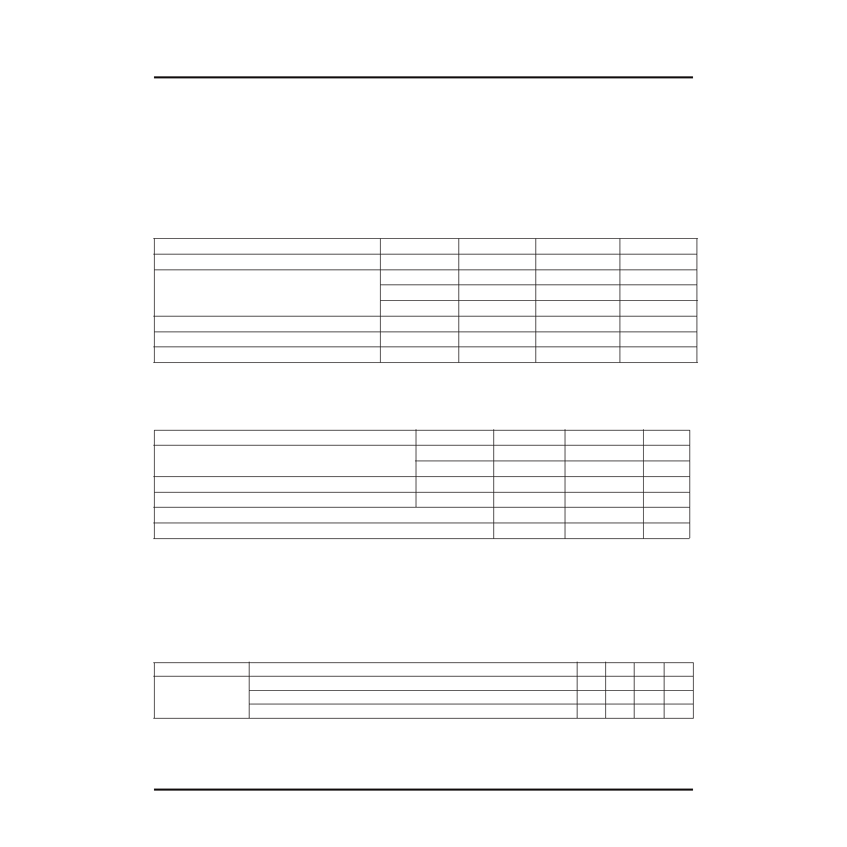
Table 23. Absolute Maximum Ratings
Recommended Operating Conditions
Table 24. Recommended Operating Conditions
*For FPGA Recommended Operating Conditions and Electrical Characteristics, see Recommended Operating Conditions and Electrical Char-
acteristics tables in the Series 4 FPGA Data Sheet and the Series 4 I/O Buffer Application Note. FPSC Standby Currents (IDDSB15 and
IDD
SB33 are tested with the Embedded Core in the powered down state
Designed for greater than 10 year electromigration life at 3.125 Gbits/s at 100 C junction temperature.
Note: VDDIB is the center tap of the CML input buffer. In some cases this signal may be left oating, or tied to another voltage level when not
interfacing to CML output buffers. See the SERDES CML Buffer Interface Technical Note for details.
SERDES Electrical and Timing Characteristics
Table 25. Maximum Power Dissipation
Parameter
Symbol
Min
Max
Unit
Storage Temperature
Tstg
– 65
150
°C
Power Supply Voltage with Respect to Ground
VDD33
– 0.3
4.2
V
VDDIO
– 0.3
4.2
V
VDD15
– 0.3
2.0
V
Input Signal with Respect to Ground
VIN
VSS – 0.3
VDDIO + 0.3
V
Signal Applied to High-impedance Output
—
VSS – 0.3
VDDIO + 0.3
V
Maximum Package Body (Soldering) Temperature
—
220
°C
Parameter
Symbol
Min
Max
Unit
Power Supply Voltage with Respect to Ground*
VDD33
3.0
3.6
V
VDD15
1.425
1.575
V
Input Voltages
VIN
VSS – 0.3
VDDIO + 0.3
V
Junction Temperature
TJ
– 40
125
°C
SERDES VDD15 Supply Voltage (VDDRx, VDDTx, VDDAUX, VDDGB)
1.425
1.575
V
SERDES CML I/O Supply Voltage (VDDIB, VDDOB)
1.425
1.890
V
Parameter
Conditions
Min
Typ
Max
Unit
Power Dissipation
SERDES, MUX/DEMUX, Align FIFO, and I/O (per channel) 1.25 Gbits/s
—
195
mW
SERDES, MUX/DEMUX, Align FIFO, and I/O (per channel) 2.5 Gbits/s
225
mW
Scrambler and Cell Processing Logic (per channel)
—
50
mW
相关PDF资料 |
PDF描述 |
|---|---|
| M-ORSO82G52BM680-DB | FPGA, 1296 CLBS, 333000 GATES, PBGA680 |
| M-ORT82G51BM680-DB | FPGA, 1296 CLBS, 333000 GATES, PBGA680 |
| M-ORT82G52BM680-DB | FPGA, 1296 CLBS, 333000 GATES, PBGA680 |
| M.PI-1R1D12 | 1 ELEMENT, 1.1 uH, GENERAL PURPOSE INDUCTOR, SMD |
| M01-014-1452PA | 14 CONTACT(S), MALE, RIGHT ANGLE TELECOM AND DATACOM CONNECTOR, SOLDER |
相关代理商/技术参数 |
参数描述 |
|---|---|
| MORTAR-44LB | 制造商:3M Electronic Products Division 功能描述:3M(TM) FIRE BARRIER MORTAR, 44 98040056073 制造商:3M Electronic Products Division 功能描述:Fire Barrier 44 lb Bag |
| MO-RX3930 | 制造商:未知厂家 制造商全称:未知厂家 功能描述:FSK RECEIVER MODULE |
| MO-RX3930-FS | 制造商:未知厂家 制造商全称:未知厂家 功能描述:FSK RECEIVER MODULE |
| MO-RX3930-FS315M | 制造商:未知厂家 制造商全称:未知厂家 功能描述:FSK RECEIVER MODULE |
| MO-RX3930-FS434M | 制造商:未知厂家 制造商全称:未知厂家 功能描述:FSK RECEIVER MODULE |
发布紧急采购,3分钟左右您将得到回复。